Manufacturing method of LED display module for splicing

A technology for display modules and manufacturing methods, which is applied in the direction of instruments, identification devices, etc., and can solve the problems affecting the uniformity of the Mini-LED display, the display effect of the Mini-LED display, the stability and service life of the Mini-LED, and the Mini-LED display airtightness and other issues to achieve the effect of ensuring the uniformity of light emission, improving the bonding force, and increasing the contact area

Pending Publication Date: 2022-04-15
SHENZHEN JUFEI OPTOELECTRONICS CO LTD
View PDF12 Cites 1 Cited by
  • Summary
  • Abstract
  • Description
  • Claims
  • Application Information

AI Technical Summary

Problems solved by technology

The high-resolution Mini-LED display needs to be realized through a small-pitch Mini-LED light-emitting unit array. Therefore, when splicing multiple Mini-LED modules, the splicing seam needs to be reduced as much as possible, and the smaller the splicing seam, the smaller the outer Mini-LED module. -The closer the LED light-emitting unit is to the splicing seam, although in the prior art, a layer of light-transmitting packaging adhesive layer is molded on the Mini-LED light-emitting unit, the light-emitting packaging layer and the substrate of the Mini-LED module are installed There may still be tiny gaps between the surface of the unit array, and because the light-emitting unit is very close to the splicing seam, the path from the light-emitting unit to the outer edge is very short, and water vapor can easily enter the Mini-LED light-emitting unit from the tiny gap at the splicing. In the chip, it affects the airtightness of the Mini-LED display, and affects the stability and service life of the Mini-LED; and if two Mini-LED modules are spliced ​​together in order to prolong the path of water vapor entering the Mini-LED light-emitting unit Increasing the distance to increase the contact surface between the light-transmitting encapsulation layer and the substrate will affect the luminous uniformity of the Mini-LED display and the display effect of the spliced ​​Mini-LED display

Method used


Image

  • Manufacturing method of LED display module for splicing
  • Manufacturing method of LED display module for splicing
  • Manufacturing method of LED display module for splicing

Examples


Embodiment 1

[0056] The invention provides a method for making a LED display module for splicing, which includes the following steps,

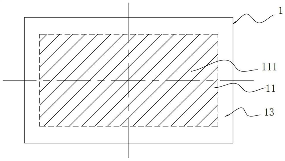
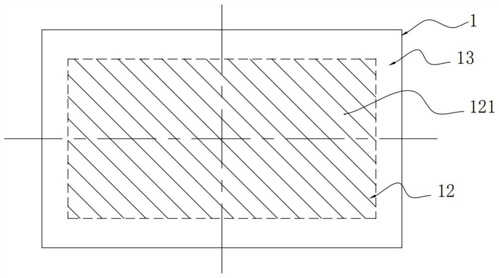
[0057] Step a: provide a substrate 1, the substrate 1 includes a front surface 11 ( figure 1 shown) and the back side 12 opposite to the front side ( figure 2 shown) and the process edge 13 located around the substrate, the display area 111 ( figure 1 The area covered by the oblique line framed by the dotted line in the center). In this embodiment, the substrate 1 is a rectangular substrate, and the front side 11 and the back side 12 are both flat. figure 1 The middle process side surrounds the four sides of the display area 111. In other embodiments, according to actual conditions and processing requirements, the process side 13 can also surround one or two opposite or adjacent sides of the display area 111. The present invention There is no limitation here. In other embodiments, the substrate 1 can also be other polygonal substrates, such as triangl...

Embodiment 2

[0071] Embodiment 2 of the present invention provides another method for manufacturing an LED display module for splicing, including the following steps:

[0072] Step A: provide a substrate, the substrate includes a front surface, a back surface opposite to the front surface, and a process edge located around the substrate, and a display area for installing a light-emitting unit is defined on the front surface; in this embodiment Step A is the same as Step a in Embodiment 1. You can refer to the description of Step a in Embodiment 1 above, and this embodiment will not repeat it here.

[0073] Step B: opening a groove around the process edge adjacent to the display area, wherein the groove does not penetrate the substrate, and the depth of the groove is greater than the thickness of the substrate that does not penetrate; Step B in this embodiment is the same as step b in Embodiment 1, and reference may be made to the description of Step b in Embodiment 1 above, and details wil...

Embodiment 3

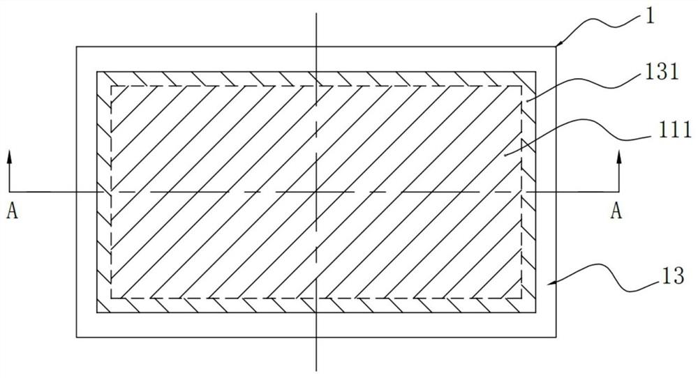
[0082] refer to Figure 21 , in this embodiment, different from the second embodiment, in step B of the second embodiment, the groove is opened around the display area 111 (refer to image 3 shown), that is, the groove 131 is opened on the front surface 11 of the substrate. In this embodiment, the groove 134 is opened on the back surface 12 of the substrate. refer to Figure 22 After molding the first transparent encapsulation layer, part of the process edge is cut off from the groove 134 , and then the second transparent encapsulation layer 153 is molded. In this embodiment, the water vapor path is extended to be flush with the back surface 12 of the substrate 1 , which is longer than the water vapor path of the LED display module provided in Embodiment 1, and the second light-transmitting encapsulant 152 is more closely bonded to the substrate 1 .

[0083] Since there is no light-emitting unit 141 installed on the back 12 of the substrate 1, and if the driving electronic ...


PUM

PropertyMeasurementUnit
thicknessaaaaaaaaaa
particle diameteraaaaaaaaaa

Abstract

The invention provides a manufacturing method of an LED display module for splicing, which comprises the following steps of: providing a substrate, arranging a process edge around the substrate, and defining a display area for mounting a light-emitting unit on the front surface of the substrate; defining a drive mounting area for mounting an electronic drive element on the back surface of the substrate; a groove which does not penetrate through the substrate is formed in the process edge, and the depth of the groove is larger than the thickness of the part, not penetrating through the substrate, of the substrate; mounting a light-emitting unit array on the display area; a light-transmitting packaging adhesive layer covering the display area is molded on the substrate, and the groove is filled with the light-transmitting packaging adhesive layer; and cutting off part of the process edge and part of the light-transmitting packaging adhesive layer along one side of the process edge to form a cutting surface on the outer side of the LED display module, and enabling the distance from the central point of the light-emitting unit closest to the cutting surface on the plane where the display area is located to the cutting surface to be smaller than or equal to 1 / 2 of the line spacing value between two rows of light-emitting units parallel to the cutting surface. The spliced display screen has the beneficial effects that water vapor invasion is prevented, and the spliced display screen is uniform in light emitting.

Description

technical field [0001] The invention relates to the field of LED displays, in particular to a method for manufacturing an LED display module used for splicing. Background technique [0002] Because Mini-LED can achieve ultra-thin, and at the same time is a small-size chip product, it can achieve high resolution, and its display effect is comparable to OLED products. When making some large-size Mini-LED displays, it is impossible to make a single large-size Mini-LED display product, and more pieces of Mini-LED modules are used for splicing to form a large-size Mini-LED display. [0003] The Mini-LED module usually includes a substrate, a Mini-LED light-emitting unit array mounted on the substrate, and a light-transmitting encapsulation layer molded on the light-emitting unit array. The high-resolution Mini-LED display needs to be realized through a small-pitch Mini-LED light-emitting unit array. Therefore, when splicing multiple Mini-LED modules, the splicing seam needs to b...

Claims


Application Information

Patent Timeline
Patent Type & Authority Applications(China)
IPC IPC(8): G09F9/302G09F9/33
Inventor 邢美正马文波李壮志
Owner SHENZHEN JUFEI OPTOELECTRONICS CO LTD
Why Eureka
Try Eureka