Touch display panel and display device

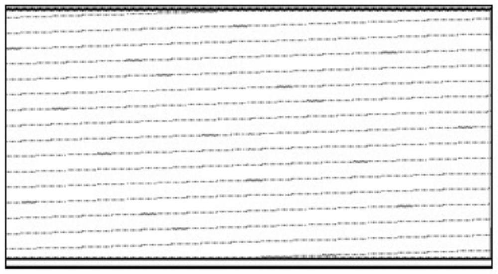
A touch display panel and touch electrode technology, applied in optics, instruments, electrical digital data processing, etc., can solve problems affecting user experience, abnormal visual effect, prone to twill, etc., to improve user experience and improve twill abnormality Circumstances, the effect of reducing differences

Pending Publication Date: 2022-04-19
XIAMEN TIANMA MICRO ELECTRONICS
View PDF7 Cites 0 Cited by
  • Summary
  • Abstract
  • Description
  • Claims
  • Application Information

AI Technical Summary

Problems solved by technology

[0003] At present, IPS LCD screens are prone to diagonal stripes under low grayscale visual effects, causing abnormal visual effects and affecting user experience

Method used


Image

  • Touch display panel and display device
  • Touch display panel and display device
  • Touch display panel and display device

Examples


no. 1 example

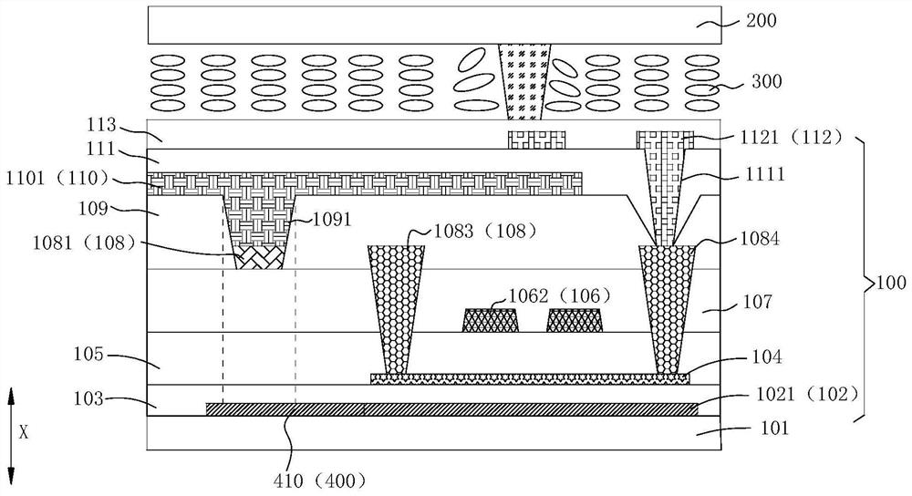
[0059] Please continue to refer to image 3 and Figure 4 , the first substrate 100 further includes a metal light shielding layer 102 , a semiconductor layer 104 , a first metal layer 106 and a second metal layer 108 . The metal light-shielding layer 102 includes a plurality of metal light-shielding blocks 1021 , the first metal layer 106 includes gate lines 1061 , and the second metal layer 108 includes a plurality of touch signal lines 1081 . The metal light shielding layer 102 is located between the first substrate 101 and the semiconductor layer 104 , and the first metal layer 106 is located between the semiconductor layer 104 and the second metal layer 108 . The first sub-shading functional block 410 is formed on the metal light-shielding layer 102, and / or, the first sub-shading functional block 410 is formed on the first metal layer 106 (as follows Figure 7 shown).

[0060] Wherein, the metal light-shielding layer 102 , the semiconductor layer 104 , the first metal ...

no. 2 example

[0098] Figure 12 It is another structural schematic diagram of the touch display panel of the present application, Figure 13 yes Figure 12 A schematic plan view of a part of the film layer of the touch display panel shown.

[0099] see Figure 12 and Figure 13 , in some optional implementation manners, the first sub-light-shielding functional block 410 is disposed on the same layer as the touch signal line 1081 and connected to the touch signal line 1081 .

[0100] The first sub-light-shielding functional block 410 is formed on the second metal layer 108 and connected to the touch signal line 1081 , which does not increase the film thickness and is easy to manufacture. Moreover, the first sub-light-shielding functional block 410 is connected to the touch signal line 1081 , which can prevent the separately deposited first sub-light-shielding functional block 410 from generating an uncontrollable potential due to capacitive coupling, which will have a negative impact on ...

no. 3 example

[0111] Figure 14 It is another structural schematic diagram of the touch display panel of the present application, Figure 15 It is another structural schematic diagram of the touch display panel of the present application, Figure 16 It is another structural schematic diagram of the touch display panel of the present application.

[0112] Please refer to Figure 14 , in some optional embodiments, a black matrix layer 201 is formed on the side of the second substrate 200 facing the first substrate 100 , and the second sub-light-shielding functional block 420 is formed on the black matrix layer 201 .

[0113] Wherein, the black matrix layer 201 includes a plurality of black matrix blocks. Its orthographic projection on the first substrate 101 mainly covers the non-light-emitting area, that is, covers metal lines such as data lines, gate lines 1061 , and touch signal lines 1081 . The material of the black matrix block is mainly dark metal or resin material, the main functio...


PUM


Abstract

The invention provides a touch display panel and a display device.The touch display panel comprises a first substrate and a second substrate which are oppositely arranged, and the first substrate comprises a first substrate body, a second substrate body and a third substrate body; a plurality of touch signal lines; the touch electrode layer comprises a plurality of touch electrode blocks arranged in an array, and each touch electrode block is connected to at least one touch signal line through a via hole; the touch display panel further comprises a shading function block which is arranged corresponding to at least part of the via holes, and the orthographic projection of the shading function block on the first substrate in the thickness direction of the touch display panel at least partially covers the orthographic projection of the via holes on the first substrate. According to the touch display panel provided by the invention, the situation of abnormal visual effect caused by twill of the touch display panel under the low-gray-scale visual effect is improved, and the user experience is improved.

Description

technical field [0001] The present application relates to the field of display technology, in particular to a touch display panel and a display device. Background technique [0002] In-Plane Switching (IPS) liquid crystal displays have attracted widespread attention due to their wide viewing angle characteristics in applications. Today, IPS mode LCDs are widely used in mobile phones, portable devices and other fields. [0003] At present, IPS LCD screens are prone to diagonal lines under low grayscale visual effects, causing abnormal visual effects and affecting user experience. Contents of the invention [0004] Embodiments of the present application provide a touch display panel and a display device, so as to improve the abnormal visual effect caused by diagonal lines appearing on a liquid crystal display screen under low gray scale visual effect. [0005] In a first aspect, an embodiment of the present application provides a touch display panel, including a first subs...

Claims


Application Information

Patent Timeline
Patent Type & Authority Applications(China)
IPC IPC(8): G06F3/041G06F3/044G02F1/1333
CPCG06F3/0412G06F3/0445G06F3/0446G02F1/13338G02F1/1333
Inventor 杨俊杰王志杰赖国昌
Owner XIAMEN TIANMA MICRO ELECTRONICS
Why Eureka
Try Eureka