Method, device and chip for transmitting pulse event

An event and pulse technology, applied in digital computer components, physical implementation, instruments, etc., can solve the problem of high power consumption, achieve the effect of reducing power consumption, high flexibility, and improving signal quality

Active Publication Date: 2022-04-19
SHENZHEN SYNSENSE TECH CO LTD +1
View PDF5 Cites 2 Cited by
  • Summary
  • Abstract
  • Description
  • Claims
  • Application Information

AI Technical Summary

Problems solved by technology

At the same time, the realization of ultra-low power consumption of brain-like chips is the unanimous pursuit of engineers. The existing processing chips need to consume a lot of power to access the memory after receiving the input pulse signal, and even some noise will wake up the processing chips to work.

Method used


Image

  • Method, device and chip for transmitting pulse event
  • Method, device and chip for transmitting pulse event
  • Method, device and chip for transmitting pulse event

Examples


Embodiment Construction

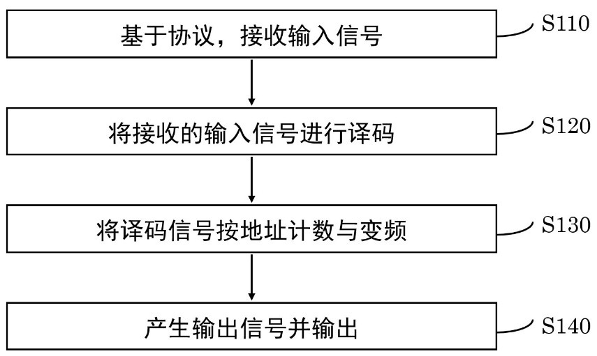
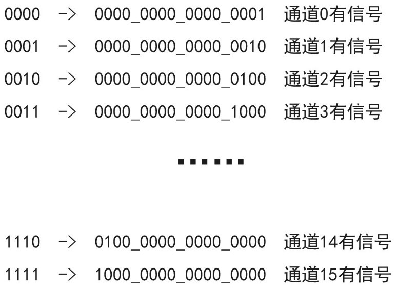
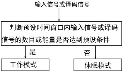
[0070] Since various alternative solutions cannot be exhaustively described, the main points of the technical solutions in the embodiments of the present invention will be clearly and completely described below in conjunction with the drawings in the embodiments of the present invention. For other technical solutions and details not disclosed in detail below, they generally belong to the technical goals or technical features that can be achieved by conventional means in this field. Due to space limitations, the present invention does not introduce them in detail.

[0071] Unless it is the meaning of division, " / " at any position in the present invention means logical "or". The "first", "second" and other serial numbers in any position of the present invention are only used for distinguishing marks in the description, and do not imply an absolute order in time or space, nor do they imply that the terms with this serial number are the same as those with the The same terms of oth...


PUM


Abstract

In order to improve the communication efficiency between chips/modules and reduce the power consumption as much as possible, the invention converts an address event expression signal into a serial address event expression signal, and comprises the following steps: receiving an input signal based on a protocol; decoding the received input signal to obtain a decoded signal; carrying out counting and frequency conversion on the decoding signals according to addresses; and generating and outputting an output signal according to the frequency-converted signal. Compared with the prior art, the interface system provided by the invention has multiple modes, can filter some noise or too slight invalid signals and improve signal quality while reducing power consumption, and has better reliability and flexibility and lower cost and power consumption. The method is suitable for the field of Internet of Things, and is especially suitable for the field of brain-like chips.

Description

technical field [0001] The present invention relates to a method, device and chip for transmitting pulse events, in particular to a method, device and chip for transmitting pulse events during communication between brain-inspired chips or modules. Background technique [0002] Address Event Representation (AER) is used for communication between neuromorphic chips (also known as brain-like chips or neuromorphic chips) or between internal modules of the chip, and additional handshake lines (confirmation and request) are used to complete asynchronous communication . In the AER protocol, events (also called pulses in this invention) are transmitted through a high-speed digital parallel bus. When the front-end chip or sensor generates an output pulse, the AER encoder assigns a digital address to the pulse, and the information is routed through the bus. to the target chip, and by analyzing the digital address, the front-end chip is able to send a pulse to any target neuron in the...

Claims


Application Information

Patent Timeline
Patent Type & Authority Applications(China)
IPC IPC(8): G06F15/163G06N3/04G06N3/063
CPCG06F15/163G06N3/049G06N3/063
Inventor 白鑫刘浩张华秋周凯乔宁
Owner SHENZHEN SYNSENSE TECH CO LTD
Why Eureka
Try Eureka