
Enhanced FVF circuit

An enhanced circuit technology, applied in the direction of adjusting electrical variables, instruments, control/regulation systems, etc., to achieve the effect of increasing power consumption, reducing output resistance, and improving loop gain

Inactive Publication Date: 2022-04-22
UNIV OF ELECTRONICS SCI & TECH OF CHINA
View PDF5 Cites 0 Cited by
  • Summary
  • Abstract
  • Description
  • Claims
  • Application Information

AI Technical Summary

Problems solved by technology

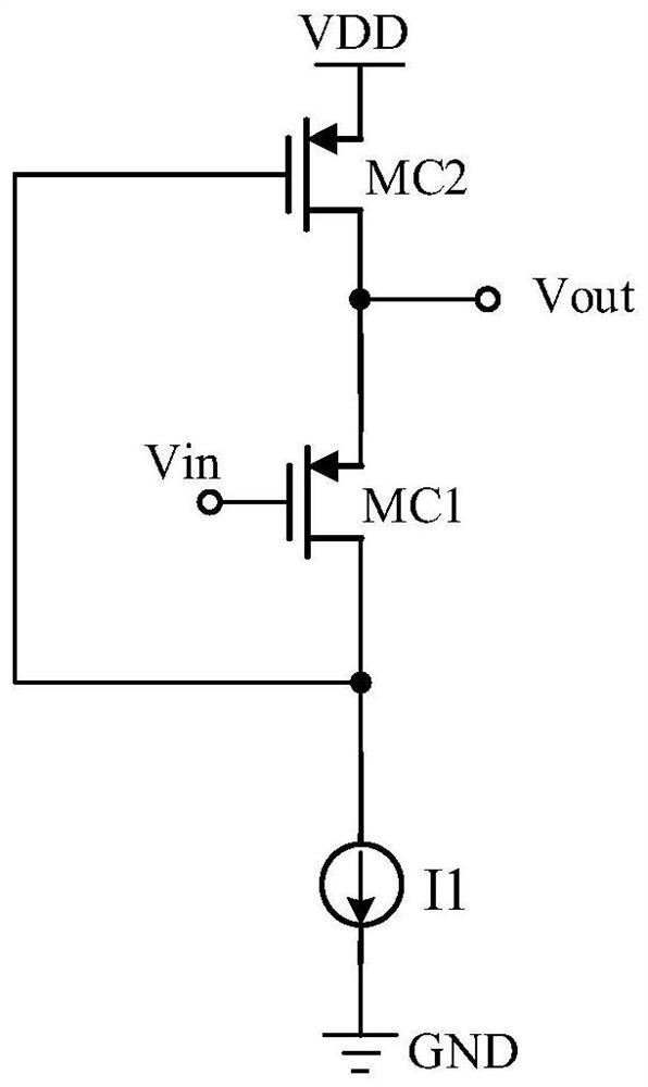
Compared with the output resistance of the traditional source follower, the traditional FVF circuit reduces the output resistance several times to dozens of times through the local negative feedback structure, but in some occasions, lower output resistance is required to achieve better performance

Method used


Image

  • Enhanced FVF circuit
  • Enhanced FVF circuit
  • Enhanced FVF circuit

Examples


Embodiment Construction

[0017] Describe technical scheme of the present invention in detail below in conjunction with accompanying drawing:

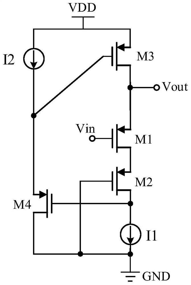
[0018] The enhanced FVF circuit of the present invention includes a first transistor M1, a second transistor M2, a third transistor M3, a fourth transistor M4, a first current source I1, and a second current source I2, wherein: the source of the first transistor M1 is connected to the second transistor M1 The drain of the third transistor M3 is used as an output terminal, the drain is connected to the source of the second transistor M2, and the gate is connected to the input; the source of the second transistor M2 is connected to the drain of the first transistor M1, and the drain is connected to the first current source I1 The positive end of the gate is grounded; the source of the third transistor M3 is connected to the power supply, the drain is connected to the source of the first transistor M1 as an output terminal, the gate is connected to the source of th...


PUM


Abstract

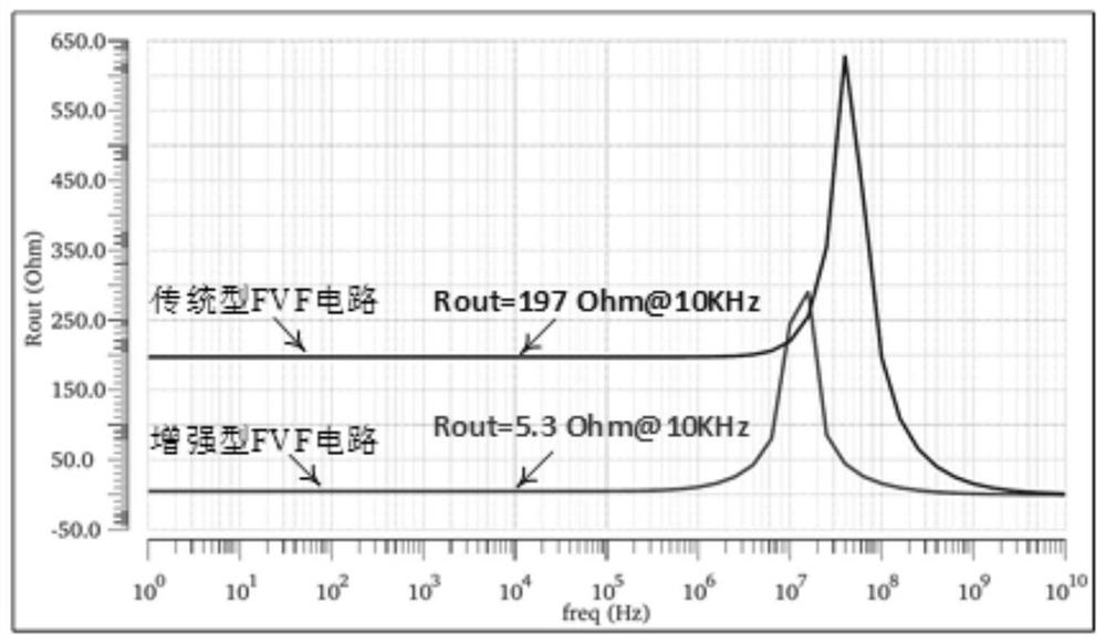
The invention belongs to the technical field of electronic circuits, and particularly relates to an enhanced FVF circuit. Compared with a traditional FVF circuit, the circuit has lower output impedance, and compared with the traditional FVF circuit, the circuit complexity is not increased. The enhanced FVF circuit can be used for an operational amplifier output stage, a linear voltage regulator circuit, some circuits needing low output impedance and the like. According to the invention, the cascode tube and the PMOS follower are added to improve the loop gain, lower output impedance is realized, the input end of the added cascode tube is constantly grounded, and additional bias voltage is avoided. The enhanced FVF circuit has a simple and effective structure, so that the enhanced FVF circuit has a wide application scene.

Description

technical field [0001] The invention belongs to the technical field of electronic circuits, and in particular relates to an enhanced FVF circuit. Background technique [0002] Traditional FVF structure such as figure 1 As shown, its principle is to reduce the output resistance of the follower through Shunt-Shunt negative feedback, and its output resistance can be expressed as [0003] [0004] g in formula (1) MC1 is the transconductance of transistor MC1, g MC2 is the transconductance of transistor MC2, r oMC1 Small-signal output resistor for MC1. Compared with the output resistance of the traditional source follower, the traditional FVF circuit reduces the output resistance several times to dozens of times through the local negative feedback structure, but in some occasions, lower output resistance is required to achieve better performance. Contents of the invention [0005] In view of the above problems, the present invention proposes an enhanced FVF circuit str...

Claims


Application Information

Patent Timeline
Patent Type & Authority Applications(China)
IPC IPC(8): G05F3/26
CPCG05F3/26
Inventor 唐鹤熊兴
Owner UNIV OF ELECTRONICS SCI & TECH OF CHINA
Learn More