Plasma processing device and working method thereof

A plasma and processing device technology, which is applied in the field of ion plasma processing devices, can solve problems such as time-consuming, long-process, and cumbersome, and achieve the effects of cost saving, easy maintenance, and improved accuracy

Pending Publication Date: 2022-05-06
ADVANCED MICRO FAB EQUIP INC CHINA
View PDF14 Cites 0 Cited by
  • Summary
  • Abstract
  • Description
  • Claims
  • Application Information

AI Technical Summary

Problems solved by technology

However, every time the cavity is opened, the staff needs to re-adjust the various components in the vacuum reaction cavity, which takes a long time and will take up a long working time of the plasma processing device and the process is cumbersome

Method used


Image

  • Plasma processing device and working method thereof
  • Plasma processing device and working method thereof
  • Plasma processing device and working method thereof

Examples


Embodiment Construction

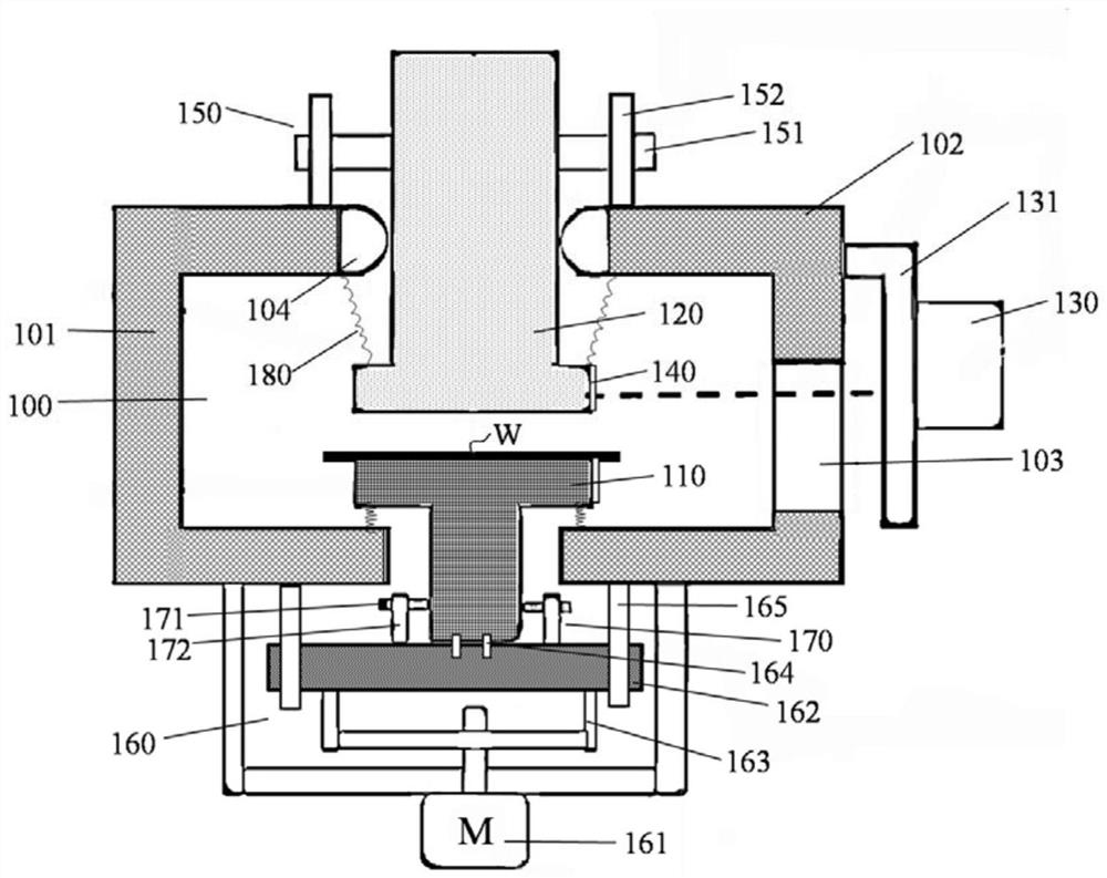
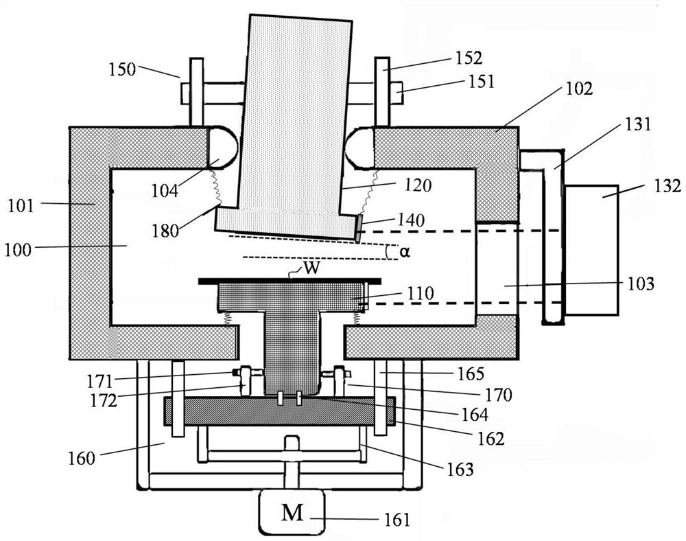
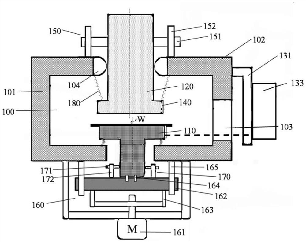
[0057]In order to make the purpose, technical solutions and advantages of the embodiments of the present invention clearer, the technical solutions in the embodiments of the present invention will be clearly and completely described below in conjunction with the drawings in the embodiments of the present invention. Obviously, the described embodiments It is a part of embodiments of the present invention, but not all embodiments. Based on the embodiments of the present invention, all other embodiments obtained by persons of ordinary skill in the art without making creative efforts belong to the protection scope of the present invention.

[0058] It should be noted that, in this document, the terms "comprising", "comprising", "having" or any other variation thereof are intended to cover a non-exclusive inclusion such that a process, method, article or terminal device comprising a series of elements Not only those elements are included, but also other elements not expressly liste...


PUM


Abstract

The invention discloses a plasma processing device and a working method thereof, and the plasma processing device comprises a vacuum reaction cavity which is formed by the surrounding of a reaction cavity body and a cavity body end cover; the lower electrode assembly is arranged in the vacuum reaction cavity; the movable upper electrode assembly is arranged opposite to the lower electrode assembly, and a plasma environment is formed between the movable upper electrode assembly and the lower electrode assembly; the reaction cavity body is provided with a plurality of observation windows, a plurality of movable monitors are arranged outside the observation windows, and the movable monitors are used for monitoring the included angle and concentricity between the movable upper electrode assembly and the lower electrode assembly. The wafer etching observation window has the advantages that the observation window is combined with the movable monitor, the structure is simple, observation is convenient, daily maintenance and use of workers are facilitated, and the wafer etching effect is further guaranteed.

Description

technical field [0001] The invention relates to the field of semiconductor equipment, in particular to a plasma processing device and a working method thereof. Background technique [0002] In the production process of semiconductor chips, a large amount of micro-processing is required, and a common method is to use a plasma processing device to process semiconductor wafers using the principle of its vacuum reaction chamber. During the entire process, the levelness and neutrality between the upper electrode assembly and the lower electrode assembly of the plasma processing device have a great influence on the etching effect of the wafer. [0003] In the field of wafer etching, such as the field of wafer edge etching, the structure of the movable upper electrode assembly is mostly used in the existing plasma processing apparatus. When the wafer is transported into and out of the vacuum reaction chamber, the upper electrode assembly is lifted; when the wafer is processed, the...

Claims


Application Information

Patent Timeline
Patent Type & Authority Applications(China)
IPC IPC(8): H01J37/32H01L21/67
CPCH01J37/3288H01J37/32568H01L21/67069H01J2237/334
Inventor 王明明黄允文吴狄杨金全
Owner ADVANCED MICRO FAB EQUIP INC CHINA
Why Eureka
Try Eureka