Supercharge Your Innovation With Domain-Expert AI Agents!

Millimeter wave PCB antenna structure

A PCB antenna and millimeter-wave technology, applied in the field of millimeter-wave PCB antenna structure, can solve the problems of difficulty in realizing millimeter-wave dual-band dual-frequency structure and dual-polarized radiation characteristics, high difficulty in antenna fabrication, and inconvenience in use, and achieve excellent performance. , high practicability, easy to use effect

Pending Publication Date: 2022-05-06
PULSE (SUZHOU) WIRELESS PRODUCTS CO LTD
View PDF0 Cites 0 Cited by
  • Summary
  • Abstract
  • Description
  • Claims
  • Application Information

AI Technical Summary

Problems solved by technology

[0003] For 5G small communication equipment, the size of the antenna is required to be small enough, and the radiation performance of the antenna is good, and the manufacturing process is required to be simple. However, the existing antenna is difficult to manufacture, and it is difficult to realize the millimeter-wave dual-band dual-frequency structure and dual Polarized radiation characteristics, more inconvenient to use

Method used


Image

  • Millimeter wave PCB antenna structure
  • Millimeter wave PCB antenna structure
  • Millimeter wave PCB antenna structure

Examples


Embodiment Construction

[0026] The following will clearly and completely describe the technical solutions in the embodiments of the present invention with reference to the accompanying drawings in the embodiments of the present invention. Obviously, the described embodiments are only some, not all, embodiments of the present invention. Based on the embodiments of the present invention, all other embodiments obtained by persons of ordinary skill in the art without making creative efforts belong to the protection scope of the present invention.

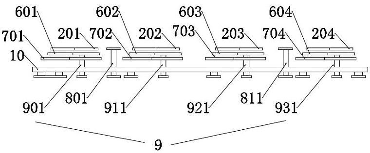
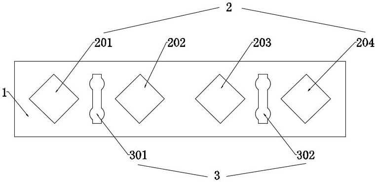
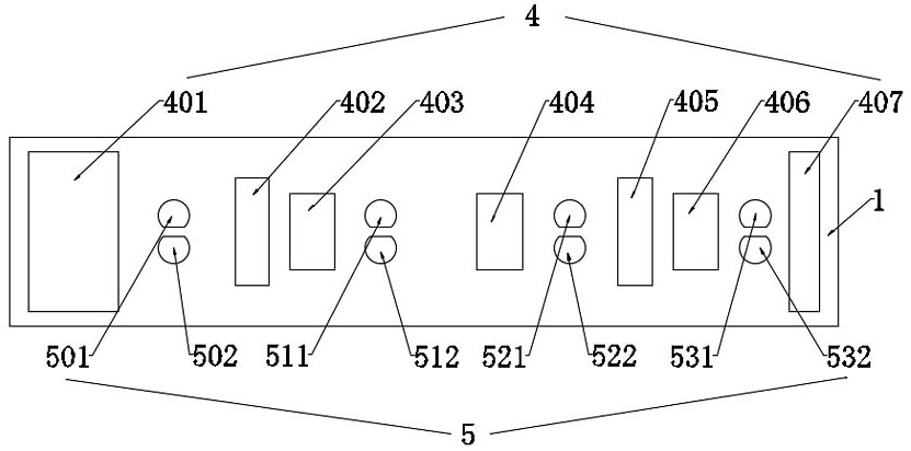
[0027] see Figure 1-10 , the present invention provides a technical solution: a millimeter-wave PCB antenna structure, including a dielectric block 1, four first-layer radiators 2 are installed on the upper surface of the dielectric block 1, and an isolation metal is fixedly connected to the upper surface of the dielectric block 1. body 3, the lower surface of the dielectric block 1 is fixedly connected with several antenna grounding metal bodies 4, and the l...


PUM


Abstract

The invention discloses a millimeter wave PCB antenna structure which comprises a dielectric block, four first-layer radiators are installed on the upper surface of the dielectric block, an isolation metal body is fixedly connected to the upper surface of the dielectric block, a plurality of antenna grounding metal bodies are fixedly connected to the lower surface of the dielectric block, and a plurality of feed contact points are fixedly connected to the lower surface of the dielectric block. The lower surface of the first-layer radiator is provided with a second-layer radiator, the lower surface of the second-layer radiator is provided with a third-layer radiator, the upper surface of the dielectric block is provided with a feed column, and the upper surface of the dielectric block is provided with a plurality of feed holes. According to the millimeter wave PCB antenna structure, the via hole is in coupling connection with the third-layer radiator and is directly connected with the second-layer radiator, the first-layer radiator and the second-layer radiator are coupled, the high-frequency bandwidth of the antenna can be increased, the manufacturing process of the antenna structure is simple, a millimeter wave band dual-frequency structure can be realized, the antenna structure has dual-polarization radiation characteristic gain, and the antenna structure is more compact. And the practicability is high.

Description

technical field [0001] The invention relates to the technical field of wireless communication, in particular to a millimeter-wave PCB antenna structure. Background technique [0002] 5G is the fifth generation of mobile communication technology. It is a new generation of broadband mobile communication technology with the characteristics of high speed, low delay and large connection. , especially the increasing application of the FR2 millimeter wave band, making the demand for corresponding 5G millimeter antennas also increasing. [0003] For 5G small communication equipment, the size of the antenna is required to be small enough, and the radiation performance of the antenna is good, and the manufacturing process is required to be simple. However, the existing antenna is difficult to manufacture, and it is difficult to realize the millimeter-wave dual-band dual-frequency structure and dual Polarized radiation characteristics, more inconvenient to use. Contents of the inven...

Claims


Application Information

Patent Timeline
Patent Type & Authority Applications(China)
IPC IPC(8): H01Q5/20H01Q5/50H01Q5/10H01Q1/38H01Q1/48H01Q1/00H01Q15/14
CPCH01Q5/20H01Q5/50H01Q1/38H01Q1/002H01Q1/48H01Q15/14H01Q5/10
Inventor 顾爱琴
Owner PULSE (SUZHOU) WIRELESS PRODUCTS CO LTD
Features
  • R&D
  • Intellectual Property
  • Life Sciences
  • Materials
  • Tech Scout
  • Unparalleled Data Quality
  • Higher Quality Content
  • 60% Fewer Hallucinations
Learn More