CMP (chemical mechanical polishing) pad and CMP device

A technology for grinding pads and grinding areas, which is applied in the direction of grinding devices, grinding machine tools, grinding tools, etc., and can solve problems that affect the uniformity of film formation patterns on wafers, excessive grinding of wafer edges, poor contact, etc.

Pending Publication Date: 2022-05-13
INST OF MICROELECTRONICS CHINESE ACAD OF SCI +1
View PDF8 Cites 1 Cited by
  • Summary
  • Abstract
  • Description
  • Claims
  • Application Information

AI Technical Summary

Problems solved by technology

After the CMP process, due to the existence of oxide residues (Oxide Residue), poor interconnection structure composed of tungsten or copper, and subsequent CMP processes, t

Method used


Image

  • CMP (chemical mechanical polishing) pad and CMP device
  • CMP (chemical mechanical polishing) pad and CMP device
  • CMP (chemical mechanical polishing) pad and CMP device

Examples


Embodiment Construction

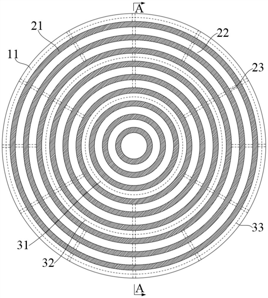
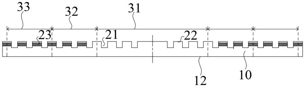
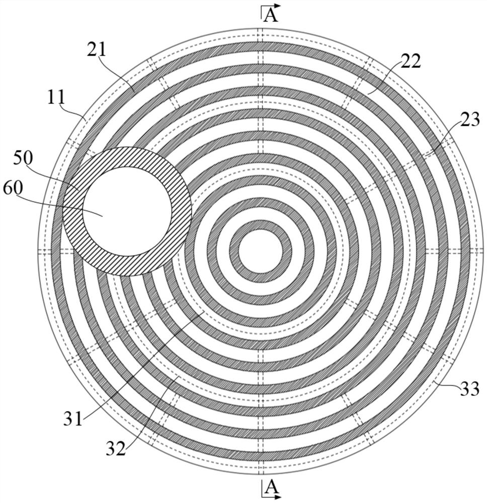
[0024] In order to make the purpose, technical solutions and advantages of the embodiments of the present invention clearer, the technical solutions in the embodiments of the present invention will be clearly and completely described below in conjunction with the drawings in the embodiments of the present invention. Obviously, the described embodiments It is only some embodiments of the present invention, but not all embodiments. Based on the embodiments of the present invention, all other embodiments obtained by persons of ordinary skill in the art without making creative efforts belong to the protection scope of the present invention.

[0025] In order to facilitate the understanding of the CMP polishing pad provided by the embodiment of the present invention, the application scene of the CMP polishing pad provided by the embodiment of the present invention is firstly described below. Structure. The CMP polishing pad will be described in detail below in conjunction with the...


PUM

PropertyMeasurementUnit
Widthaaaaaaaaaa

Abstract

The invention provides a CMP (chemical mechanical polishing) pad and a CMP device. The CMP pad comprises a disc-shaped polishing pad. The grinding pad further comprises a plurality of annular grooves formed in the grinding surface, and the annular grooves are sequentially distributed from the center of the grinding pad to the edge of the grinding pad in a concentric circle shape. The grinding surface is divided into N grinding areas. The N grinding areas comprise a first round grinding area located in the center of the grinding pad and further comprise a second grinding area to an Nth grinding area which are sequentially arranged from the center of the grinding pad to the edge of the grinding pad in a concentric circle shape. And a through hole for communicating any two adjacent circular grooves in the grinding area is formed in each grinding area from the second grinding area to the Nth grinding area in a penetrating manner. The through holes are formed in the grinding areas from the second grinding area to the Nth grinding area in the penetrating mode, the amount of grinding liquid in the different grinding areas is adjusted, the uniformity of film forming patterns on the surface of a wafer in the CMP process is improved, and the yield is increased.

Description

technical field [0001] The invention relates to the technical field of semiconductor manufacturing, in particular to a CMP polishing pad and a CMP polishing device. Background technique [0002] As the patterns designed and produced on the wafer are gradually refined, for various purposes, the CMP (Chemical Mechanical Polishing, chemical mechanical polishing) process is increasing, which can reduce the height difference at the edge of the film-forming pattern on the wafer. Therefore, the uniformity of the film formation pattern on the wafer in the CMP process becomes more important. The uniformity of the film formation pattern on the wafer in the CMP process is affected by the structure of the equipment, the mode, and the overall process. After the CMP process, due to the existence of oxide residues (Oxide Residue), poor interconnection structure composed of tungsten or copper, and subsequent CMP processes, the uniformity of the film pattern on the wafer will be affected, r...

Claims


Application Information

Patent Timeline
IPC IPC(8): B24B37/26B24B37/34H01L21/306
CPCB24B37/26B24B37/34H01L21/30625
Inventor 金泰源张月杨涛卢一泓刘青
Owner INST OF MICROELECTRONICS CHINESE ACAD OF SCI
Why Eureka
Try Eureka