Device and method for detecting surface defects of planar optical element

A technology of optical components and detection devices, which is used in measurement devices, optical testing of defects/defects, material analysis by optical means, etc., can solve the problem that the detection results are not intuitive, the detection process is cumbersome, and the specific location and size of defects cannot be accurately described. size and other problems, to eliminate power instability, improve detection accuracy, and improve detection efficiency.

Pending Publication Date: 2022-05-13
HEFEI INSTITUTES OF PHYSICAL SCIENCE - CHINESE ACAD OF SCI
View PDF0 Cites 1 Cited by
  • Summary
  • Abstract
  • Description
  • Claims
  • Application Information

AI Technical Summary

Problems solved by technology

The disadvantage is that the test results are not intuitive, and the specific location and size of the defect cannot be accurately described
[0003] In view of the above problems, it can be seen that the current inspection process of optical components is very cumbersome and full of uncertainties, so it is very important to build a simple and efficient optical component surface defect detection system

Method used


Image

  • Device and method for detecting surface defects of planar optical element
  • Device and method for detecting surface defects of planar optical element
  • Device and method for detecting surface defects of planar optical element

Examples


Embodiment Construction

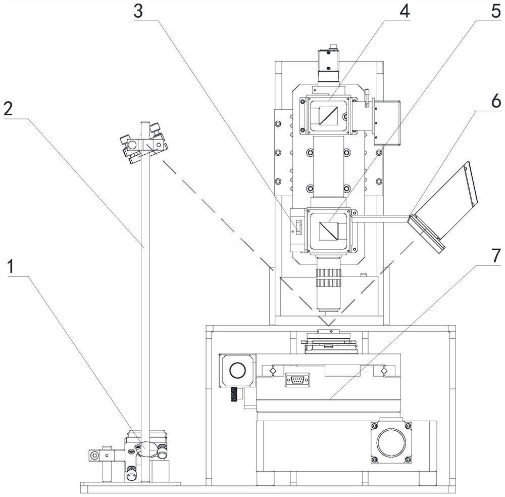
[0065] In this example, if figure 1 As shown, a surface defect detection device for a planar optical element includes: a laser 1, a beam deflection module 2, a focus measurement module 3, a main detection module 4, a main optical path module 5, an optical trap module 6, and a motion control module 7;

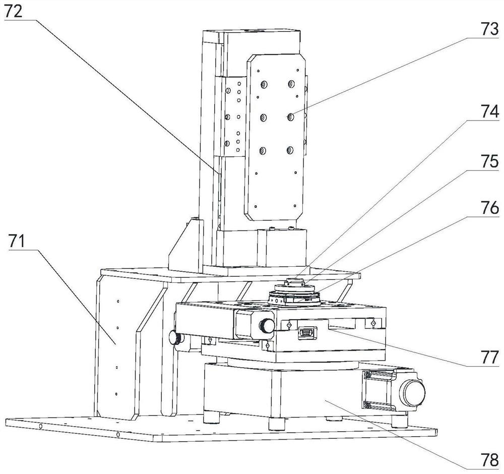
[0066] Such as figure 2 As shown; the motion control module 7 includes: a support 71, a vertical displacement stage 72, a substrate 73, a sample holder 75, an inclined stage 76, a two-dimensional displacement stage 77, and a rotary stage 78;

[0067] The sample 74 to be tested is arranged on the sample holder 75 and fixed on the tilting table 76, the tilting table 76 is fixed on the two-dimensional displacement table 77, and the two-dimensional displacement table 77 is fixed on the rotary table 78; the rotary table 78 is fixed on the support 71 ;

[0068] The base plate 73 is fixed on the vertical displacement platform 72, and the vertical displacement platform 72 is also fix...


PUM


Abstract

The invention discloses a device and a method for detecting surface defects of a planar optical element. The device comprises a laser, a light beam turning module, a focus measuring module, a main detection module, a main light path module, a light trap module and a motion control module, wherein laser emitted by the laser device is incident to the surface of a to-be-detected sample through the light beam turning module, and the light trap module is arranged on a path of reflected light of the light trap module. The microscope is arranged right above the sample to be detected and is used for receiving scattered light within a certain solid angle range; one part of the received scattered light is imaged on the CMOS, and the other part of the received scattered light is received by the PMT energy receiving module through the beam splitter prism. And the focus measuring module detects the optimal focal plane position of the sample to be measured through the other beam splitter prism. According to the invention, an imaging method and a non-imaging method are combined with each other, so that the positions and two-dimensional size information of defects can be well distinguished, the energy of scattered light generated by the defects can be obtained, the detection efficiency is further improved, and the time consumed by detection is shortened.

Description

technical field [0001] The invention belongs to the technical field of surface flaw detection of optical elements, and relates to a surface flaw detection device and a detection method of a planar optical element. Background technique [0002] Optical surface defects are mainly divided into pitting, scratches and broken edges. The most commonly used detection method is the visual method, but this method has high requirements on the observer's knowledge structure and practical experience level, and is highly subjective. Moreover, it is impossible to quantify the defect level, which is time-consuming, labor-intensive and labor-intensive. In addition, Chinese standards are different from international standards and European standards, and the specified terms, codes, and signs of optical component surface defects are different, making it difficult to form a unified standard. At present, there are many emerging surface defect detection methods, most of which are processed by th...

Claims


Application Information

Patent Timeline
Patent Type & Authority Applications(China)
IPC IPC(8): G01N21/88G01N21/01
CPCG01N21/88G01N21/01G01N2021/0112
Inventor 宋茂新陈曦李朕阳凌明椿楚玉恒管恒睿匡大鹏刘吴昊赵鑫鑫洪津
Owner HEFEI INSTITUTES OF PHYSICAL SCIENCE - CHINESE ACAD OF SCI
Why Eureka
Try Eureka