Optical packaging structure

A technology of packaging structure and optoelectronic structure, applied in the field of optical communication, can solve the problems of integrating more channels, increasing the volume of the packaging structure, etc.

Pending Publication Date: 2022-05-13
GUANGXUN SCI & TECH WUHAN
View PDF7 Cites 1 Cited by
  • Summary
  • Abstract
  • Description
  • Claims
  • Application Information

AI Technical Summary

Problems solved by technology

However, in the design of the existing optical component packaging structure, if more channels are to be integrated, it is necessary to greatly increase the volume of the packaging structure, which cannot achieve the purpose of integrating more channels in the same size space

Method used


Image

  • Optical packaging structure
  • Optical packaging structure
  • Optical packaging structure

Examples


Embodiment 1

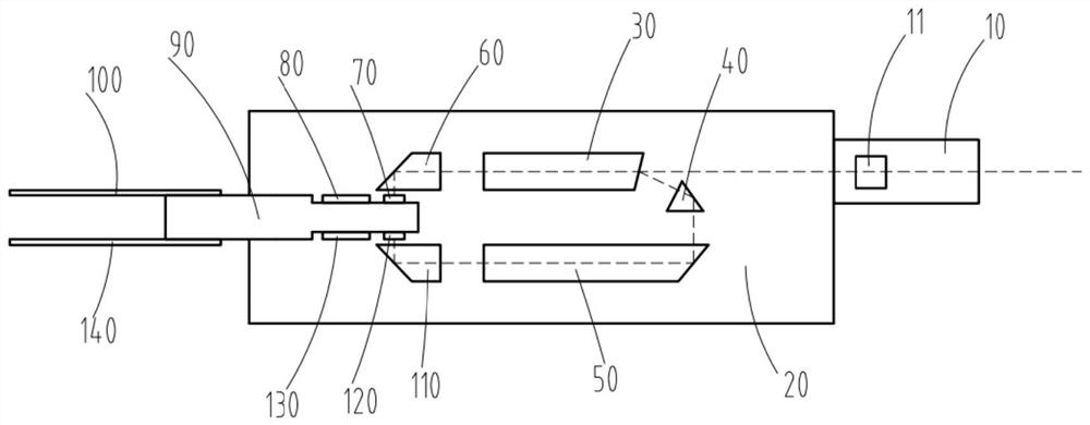
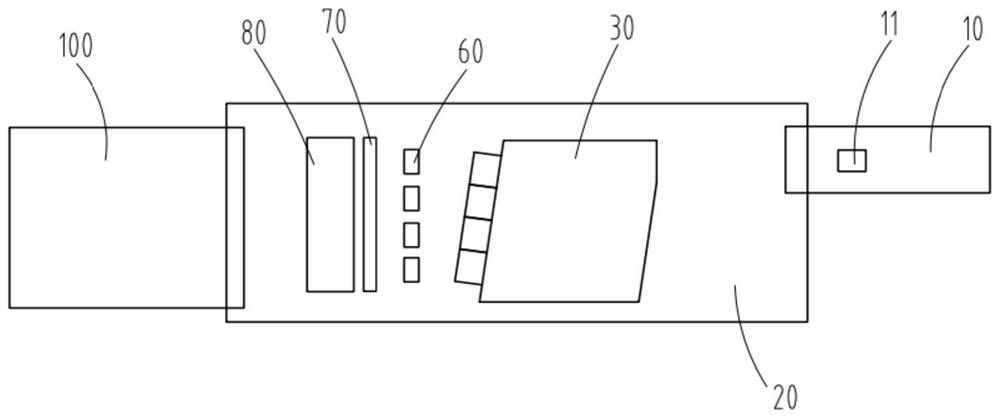
[0031] The preferred embodiment 1 of the present invention proposes an optical package structure, including an input port, an output port, and a photoelectric structure arranged in layers. , packing more optical channels. The optoelectronic structure of this embodiment is described by taking the upper and lower layers as an example. The optoelectronic structure includes a first optical part and a first electrical part arranged on the first layer, a second optical part and a second electrical part arranged on the second layer and a refraction component arranged between the first layer and the second layer, when an external optical signal is input from the input port, a part of the optical signal completes photoelectric conversion at the first electrical portion after passing through the first optical portion, Another part of the optical signal passes through the refraction component and the second optical part in turn to complete the photoelectric conversion at the second elect...

Embodiment 2

[0044] Based on the optical packaging structure provided in Embodiment 1, the manufacturing process of the optical packaging structure is described in detail in Embodiment 2 of the present invention. It should be noted that before starting the production, in order to facilitate the assembly of the upper and lower two-component wave components, the upper and lower sides of the housing 20 are open, and the housing 20 used here is in the form of a tube and shell.

[0045] refer to figure 1 Firstly, the casing 20 and the ceramic component 90 are sintered together. The ceramic component 90 has two upper and lower surfaces, and a part of the ceramic component 90 is inside the casing 20 and a part is outside the casing 20 . The electrical connection between the inside and the outside can be realized by routing wires on the back of the ceramic component 90 and the internal metal layer. In addition, in this embodiment, input and output pads are respectively provided at both ends of the...

Embodiment 3

[0055] Embodiment 3 also provides an optical packaging structure. The basic idea of ​​the packaging structure is similar to that of the optical packaging structures of Embodiment 1 and Embodiment 2. The difference is that the optical path of the optical packaging structure of Embodiment 3 is the same as that of Embodiment 1. , The optical path of embodiment 2 is opposite.

[0056] Specifically, such as Figure 7 As shown, the optical packaging structure of this embodiment 3 includes an optical path structure arranged in layers, and the optical path structure includes a first optical path structure arranged on the first layer, a second optical path structure arranged on the second layer, and a second optical path structure arranged on the first layer The light turning member 230 between the layer and the second layer, the first optical path structure includes the first group of lasers 210, the first group of turning lenses 211 and the first wave multiplexing element 212, and th...


PUM


Abstract

The invention relates to the technical field of optical communication, in particular to an optical packaging structure which comprises an input port, an output port and a photoelectric structure arranged in a laminated mode. The photoelectric structure comprises a first optical part and a first electrical part which are arranged on a first layer, a second optical part and a second electrical part which are arranged on a second layer, and a refraction component which is arranged between the first layer and the second layer. One part of the optical signal passes through the first optical part and then is subjected to photoelectric conversion at the first electrical part, and the other part of the optical signal passes through the refraction component and the second optical part in sequence and then is subjected to photoelectric conversion at the second electrical part. According to the invention, through the stacked photoelectric structure, the number of channels which can be packaged in the same space is increased, and the purpose of packaging more optical channels under the condition that the size of an optical device is basically unchanged is achieved.

Description

technical field [0001] The invention relates to the technical field of optical communication, in particular to an optical packaging structure. Background technique [0002] Optical transceiver modules, optical transmitting components and optical receiving components are all key components in optical communication systems. The development direction of existing optical modules and optical devices basically requires the integration of more channels of optical components in the same size space. However, in the design of the existing optical component packaging structure, if more channels are to be integrated, the volume of the packaging structure must be greatly increased, which cannot achieve the purpose of integrating more channels in the same size space. [0003] In view of this, how to overcome the defects in the prior art and solve the above-mentioned problem of integrating more channels in the same size space is an urgent problem to be solved in the technical field. Con...

Claims


Application Information

Patent Timeline
Patent Type & Authority Applications(China)
IPC IPC(8): G02B6/42
CPCG02B6/4206G02B6/4214G02B6/4215G02B6/4246G02B6/4287
Inventor 陈土泉史如玉顾本艳曹丽
Owner GUANGXUN SCI & TECH WUHAN
Why Eureka
Try Eureka