Single-hole double-signal double-sided backboard and manufacturing method thereof

A manufacturing method and dual-signal technology, which are applied in the directions of making wiring diagrams of printed circuits, manufacturing of printed circuits, and forming electrical connections of printed components, etc., can solve problems such as increasing the difficulty of development, increasing the weight of equipment, and prolonging the development cycle, so as to improve the node density. , to meet the needs of use, the effect of extensive use of value

Pending Publication Date: 2022-05-24
CHINA AVIATION OPTICAL-ELECTRICAL TECH CO LTD
View PDF0 Cites 0 Cited by
  • Summary
  • Abstract
  • Description
  • Claims
  • Application Information

AI Technical Summary

Problems solved by technology

[0003] With the development of miniaturization, high speed, modularization and system expansion of military electronic equipment, the interface connector nodes of the plug-in in the chassis are becoming more and more dense, but under the conditions of the original limited framework (the interface remains unchanged and the size remains unchanged) , the connector node can no longer be expanded, and cannot adapt to the situation where there are more high-speed nodes required
[0004] If it is necessary to expand the interface, the original chassis / rack size, plug-in size, and connector type must be changed, that is, the entire system is redesigned, which not only increases the development cost, but also prolongs the development cycle, increases the difficulty of development, and increases the weight of the equipment. This is very unfavorable to equipment replacement and cannot meet the requirements of model development

Method used


Image

  • Single-hole double-signal double-sided backboard and manufacturing method thereof
  • Single-hole double-signal double-sided backboard and manufacturing method thereof
  • Single-hole double-signal double-sided backboard and manufacturing method thereof

Examples


Embodiment Construction

[0035] In order to further illustrate the technical means and effects adopted by the present invention to achieve the predetermined purpose of the invention, the following describes the specific implementation, structure, Features and their effects are described in detail below.

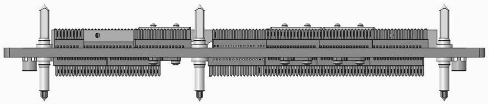
[0036] see Figure 1-4 , which is a schematic diagram of the structure of each part of the single-hole dual-signal double-sided backplane of the present invention, the single-hole dual-signal double-sided backplane includes a printed board 3, and the printed board 3 is provided with jacks 5 extending along the thickness direction. , the front board connector 1 fixed on the front face of the printed board 3 and the rear board connector 2 fixed on the rear face of the printed board 3 correspond to the printed board 3 through the pins protruding therefrom The cooperation of the jack 5 realizes the communication with the printed board 3 .

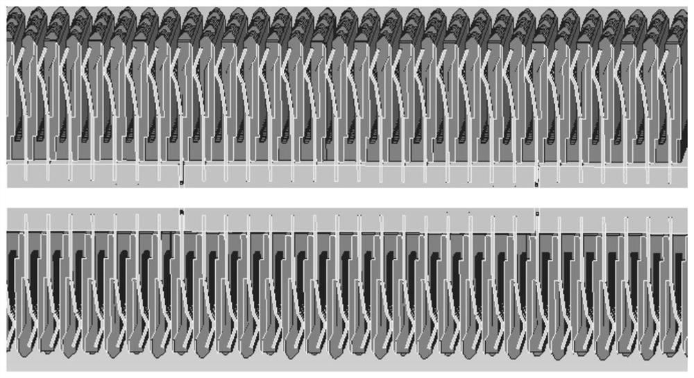
[0037] Both ends of the same socket 5 on the printed board 3 a...


PUM

PropertyMeasurementUnit
Thicknessaaaaaaaaaa

Abstract

The invention relates to a single-hole double-signal double-sided backboard and a manufacturing method thereof, the single-hole double-signal double-sided backboard comprises a printed board which is connected and matched with connector pins on the end faces of the two sides of the printed board through jacks, and each jack on the printed board is connected with two connectors at the same time. At least one jack is divided into two insertion cavities which are not communicated with each other by the separation part in the middle of the jack, and each insertion cavity is communicated with one signal layer, so that the jack can realize transmission of two signals. According to the invention, the middle part of the jack on the double-sided backboard is broken, so that signals transmitted at the two ends of the jack are not conducted, double-signal transmission can be realized by a single jack, and the node density can be improved and the use requirement can be met on the premise that the original framework is not changed.

Description

technical field [0001] The invention belongs to the technical field of double-sided backplanes, and in particular relates to a single-hole dual-signal double-sided backplane and a manufacturing method thereof. Background technique [0002] The double-sided backplane is installed in the middle of the chassis / rack, and there are daughter boards on the front and back for communication between the front board and the rear board. In the traditional backplane, the front socket and the rear socket are crimped on the backplane through the same through-hole package to realize the connection between the front socket and the rear socket, that is, the front board and the rear board share a pin for signal connection. [0003] With the development of miniaturization, high speed, modularization and system expansion of military electronic equipment, the interface connector nodes of the plug-in in the chassis are getting denser and denser, but under the conditions of the original limited fra...

Claims


Application Information

Patent Timeline
IPC IPC(8): H05K7/14H05K1/11H05K3/00H05K3/42
CPCH05K7/1438H05K7/1452H05K1/115H05K3/0005H05K3/0002H05K3/0047H05K3/42
Inventor 王淑娟夏仁善吕云朋韩茂广张玉铃李慧利
Owner CHINA AVIATION OPTICAL-ELECTRICAL TECH CO LTD
Why Eureka
Try Eureka