Backlight module and MiniLED display device

A backlight module and backplane technology, applied in the field of display screens, can solve problems such as complicated ink layer printing, non-compliance with ultra-thinness, and increased light mixing distance, so as to improve uneven brightness and darkness, shorten light mixing distance, and improve effect of effect

Active Publication Date: 2022-05-27
CHANGSHA HKC OPTOELECTRONICS CO LTD +1
View PDF6 Cites 1 Cited by
  • Summary
  • Abstract
  • Description
  • Claims
  • Application Information

AI Technical Summary

Problems solved by technology

Due to the high brightness of the center of the LED, if the dot matrix effect of the illuminant needs to be weakened, the light mixing effect needs to be enhanced, and the enhancement means that the thickness of the diffusion plate needs to be increased, and the increase in the thickness of the diffusion plate will inevitably lead to the overall thickness of the Mini LED display device. Increase, in order to avoid uneven display, generally use a thicker diffuser plate, or multiple diffuser films, and increase the light mixing distance, making the module thicker
This is not in line with the existing trend of ultra-thin Mini LED display devices. In the prior art, the ink layer is also used to enhance the light mixing effect, but the printing of the ink layer is complicated and the light mixing effect is poor.

Method used


Image

  • Backlight module and MiniLED display device
  • Backlight module and MiniLED display device
  • Backlight module and MiniLED display device

Examples


Embodiment 1

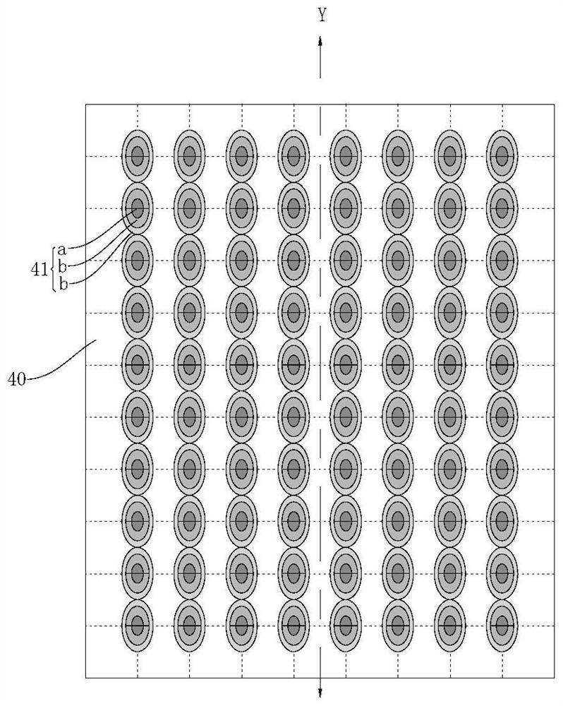
[0071] as Figure 3 and Figure 4 As shown, the first optical film layer 40 is provided with a first ink pattern 41, as shown Figure 5As shown, the second optical film layer 50 is provided with a second ink pattern 51, the center axis of the first ink pattern 41 and the center axis of the second ink pattern 51 are coincident with the central axis of the luminous body 20, the first ink pattern 41 and the second ink pattern 51 are ovals of the same size and shape, the long axis of the first ink pattern 41 is parallel to the Y axis direction, the long axis of the second ink pattern 51 is parallel to the X axis direction, and the first ink pattern 41 can be reconnected with the second ink pattern 51 by rotating 90 °. The first ink pattern 41 and the second ink pattern 51 both include a first shading region a and two second shading region b. as Figure 6 and Figure 7 As shown, after the projection superposition of the reference plane 2 forms at least three regions of different transmittan...

Embodiment 2

[0073] as Figure 9 As shown, the first optical film layer 40 is provided with a first ink pattern 41, as shown Figure 10 As shown, the second optical film layer 50 is provided with a second ink pattern 51, the central axis of the first ink pattern 41 and the central axis of the second ink pattern 51 coincide with the central axis of the luminous body 20, the first ink pattern 41 and the second ink pattern 51 are circular in the same shape but of different sizes, the size of the first ink pattern 41 is larger than the size of the second ink pattern 51, accordingly, the first ink pattern 41 and the second ink pattern 51 both include a first coloring region a and the same number of second coloring region b. The first shading region a of the first ink pattern 41, the first shading region a and the second shading region b of the first ink pattern 41 and the corresponding first shading region a and the second shading area b of the second ink pattern 51 are larger, and when the reference...


PUM


Abstract

The invention relates to a backlight module and a Mini LED display device, and belongs to the technical field of display devices.The backlight module comprises a back plate, a plurality of circuit substrates distributed in an array mode, a plurality of light-emitting bodies arranged on the circuit substrates, a diffusion plate, a first optical film layer and a second optical film layer, a first printing ink pattern is arranged at the position, corresponding to the luminous bodies, of the first optical film layer, a second printing ink pattern is arranged at the position, corresponding to the luminous bodies, of the second optical film layer, projection parts, in a reference plane, of the first printing ink pattern and the second printing ink pattern corresponding to each luminous body are overlapped, and the overlapped areas are opposite to the corresponding luminous bodies; the reference plane is parallel to the first optical film layer and/or the second optical film layer. According to the backlight module, the thickness of the diffusion plate can be correspondingly reduced, the light mixing distance is shortened, and the Mini LED display device can be wholly thinned.

Description

Technical field [0001] The present application relates to the field of display technology, in particular to a backlight module and a MiniLED display device. Background [0002] MiniLED display device is the application of MiniLED backlight technology thin film transistor liquid crystal display, generally by thousands of micro LED soldering are distributed on the circuit substrate, the current circuit substrate only supports small size, so as a large size of the backlight module, often need a plurality of circuit substrates to splice into the corresponding large size of the circuit substrate, in order to form a high-brightness uniform distribution and can be independently partitioned control of the surface light source. In order to thermally expand and contract the circuit substrate, it is often reserved for space, and there will be a gap between the two adjacent MiniLED circuit substrates, so that there will be a dark area at the seam because there is no luminous body. Due to the...

Claims


Application Information

Patent Timeline
Patent Type & Authority Applications(China)
IPC IPC(8): G02F1/13357G02F1/1335
CPCG02F1/133603G02F1/133606G02F1/133611G02F1/133512
Inventor 刘虎李荣荣
Owner CHANGSHA HKC OPTOELECTRONICS CO LTD
Why Eureka
Try Eureka