Discrete device testing method

A technology of discrete devices and testing methods, applied in semiconductor/solid-state device testing/measurement, electrical components, circuits, etc., can solve problems such as affecting chip quality and unstable test results of 300mm wafer products, achieving convenient testing and improving testing. The effect of precision and chip quality

Pending Publication Date: 2022-06-03
SHANGHAI HUAHONG GRACE SEMICON MFG CORP
View PDF0 Cites 0 Cited by
  • Summary
  • Abstract
  • Description
  • Claims
  • Application Information

AI Technical Summary

Problems solved by technology

For the 200mm wafer test, under thick wafer conditions, the DC parameter test results are consistent with the test results after thinning and packaging, and are stable; while the test results of some 300mm wafer products are unstable, and inconsistent with the test results after thinning and packaging, affecting chip quality

Method used


Image

  • Discrete device testing method
  • Discrete device testing method

Examples


Embodiment Construction

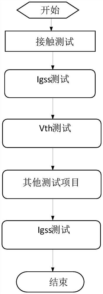
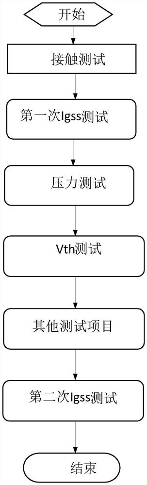
[0035] like figure 2 As shown, the discrete device testing method of the present invention comprises the following steps:

[0036] Step 1, contact test; the contact test mainly confirms whether the probe is in good contact with the pad (pin pad) of the discrete device. The contact test generally adopts the method of applying current to measure the voltage, and the test time is generally between several milliseconds to several hundred milliseconds. Testers are purchased on demand.

[0037] Step 2, the first gate-source leakage (lgss) test; apply a voltage to the gate of the discrete device according to the specifications, the drain and source are short-circuited, and the leakage current between the gate and the source is tested. Between tens of volts, the test time is generally tens of milliseconds.

[0038] Step 3, stress test; the stress test mainly applies voltage or current to the gate, drain, and source of the discrete device within a certain period of time. The applie...


PUM


Abstract

The invention discloses a discrete device testing method. The discrete device testing method comprises the following steps: step 1, contact testing; step 2, carrying out a first gate-source electric leakage test; step 3, pressure testing; 4, testing a threshold value; step 5, other test items; and step 6, carrying out a second gate-source electric leakage test. According to the invention, a stable and reliable DC parameter result can be well obtained, the test is convenient, and the test precision and the chip quality are improved.

Description

technical field [0001] The invention relates to the field of semiconductors, in particular to a method for testing discrete devices. Background technique [0002] In the field of semiconductor chip testing, for discrete device wafer testing, generally only DC items are tested. [0003] At present, the mainstream of discrete device wafers is 200mm wafers. With the demand of the market and the continuous development of technology, the number of 300mm discrete device wafer manufacturing plants is also increasing. [0004] The current DC test flow of discrete devices is as follows: figure 1 As shown, it sequentially includes a contact test, a gate-source leakage (lgss) test, a threshold voltage (vth) test, other test items, and a gate-source leakage (lgss) test. [0005] In the actual test, due to certain limitations, 300mm wafers need to use thick (not thinned) for DC parameter testing. For the 200mm wafer test, under thick wafer conditions, the DC parameter test results are...

Claims


Application Information

Patent Timeline
Patent Type & Authority Applications(China)
IPC IPC(8): H01L21/66
CPCH01L22/14H01L22/20
Inventor 谢晋春
Owner SHANGHAI HUAHONG GRACE SEMICON MFG CORP
Why Eureka
Try Eureka