Method and apparatus for Terminating A Test Signal Applied To Multiple Semiconductor Loads Under Test

a test signal and semiconductor technology, applied in the field of semiconductor testing, can solve the problems of increasing the rise and fall times of the test signal applied to the duts, design constraints, and significant cost factors of the test system controller, and achieve the effect of decreasing the rise/fall time of the test signal

Active Publication Date: 2010-10-07
FORMFACTOR INC
View PDF10 Cites 18 Cited by
  • Summary
  • Abstract
  • Description
  • Claims
  • Application Information

AI Technical Summary

Benefits of technology

[0010]Embodiments of the invention relate to a method of decreasing rise/fall time of a test signal in a semiconductor test system. In some embodiments, the method includes generating the test signal at a tester; coupling the test signal to the DUT through a signal path on and/or in a probe card assembly, the signal path having a trac

Problems solved by technology

A test system controller with increased test channels can be a significant cost factor for a test system.
In some cases, the DUTs are capacitive, which can cause an increase in th

Method used


Image

  • Method and apparatus for Terminating A Test Signal Applied To Multiple Semiconductor Loads Under Test
  • Method and apparatus for Terminating A Test Signal Applied To Multiple Semiconductor Loads Under Test
  • Method and apparatus for Terminating A Test Signal Applied To Multiple Semiconductor Loads Under Test

Examples


Embodiment Construction

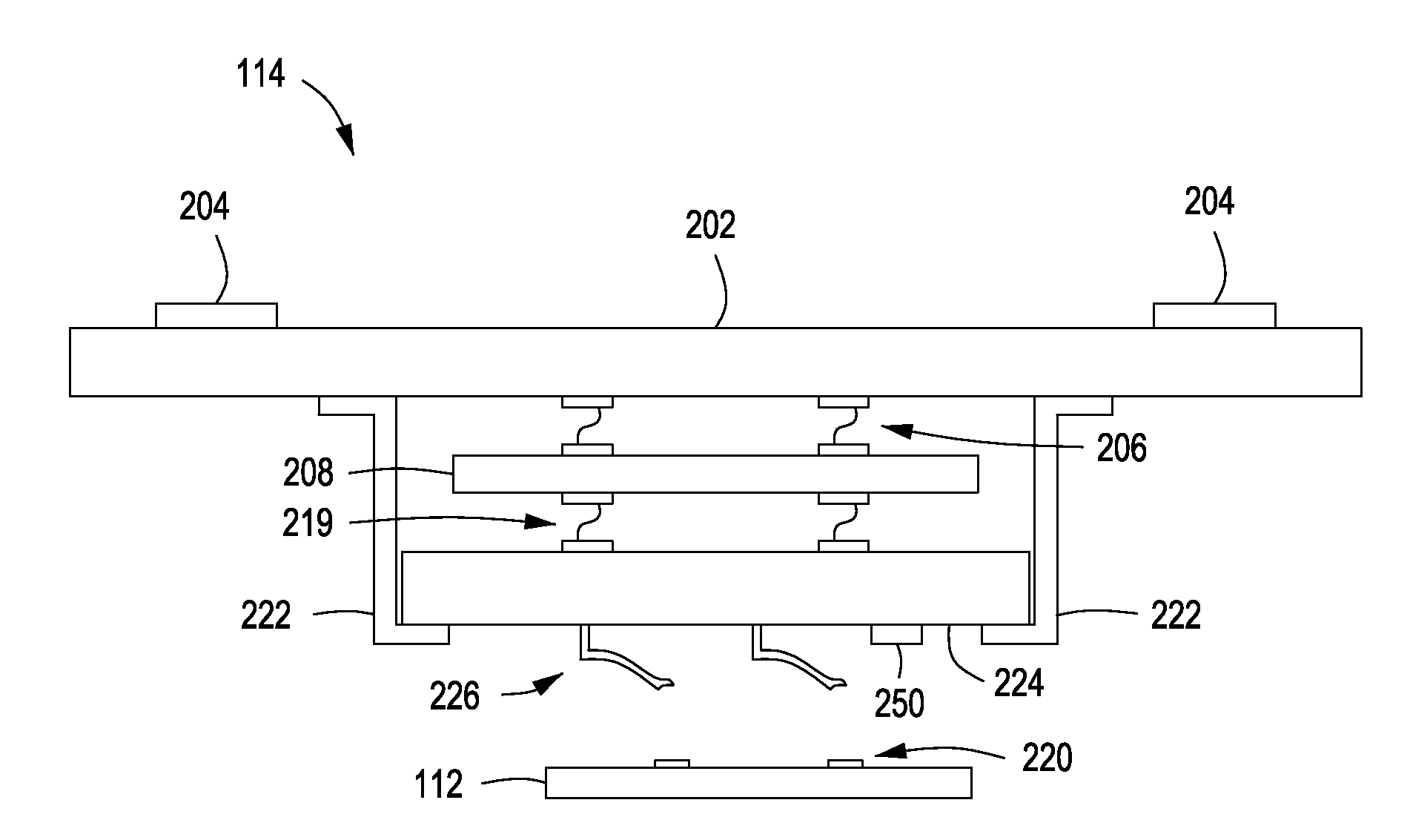
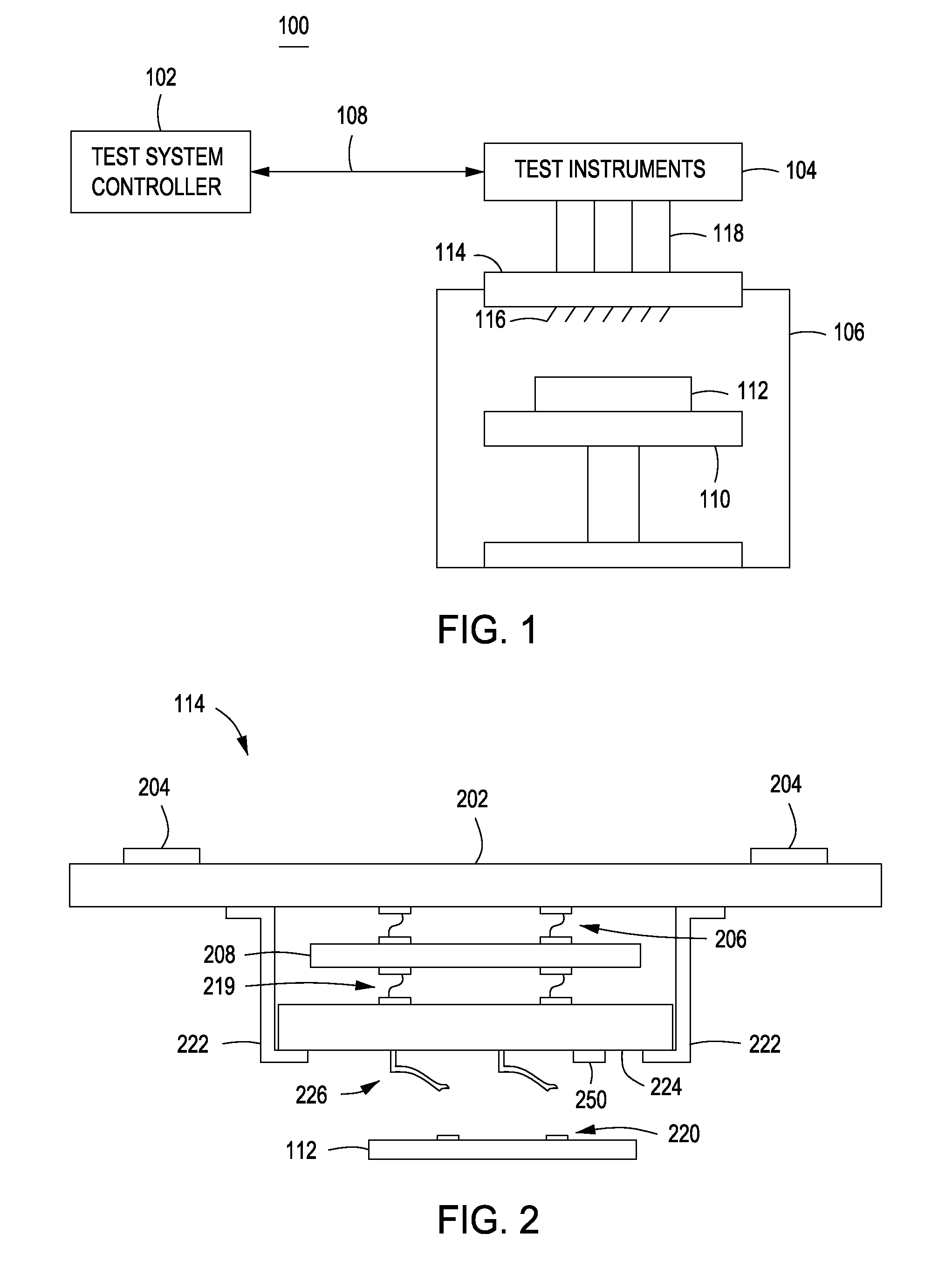
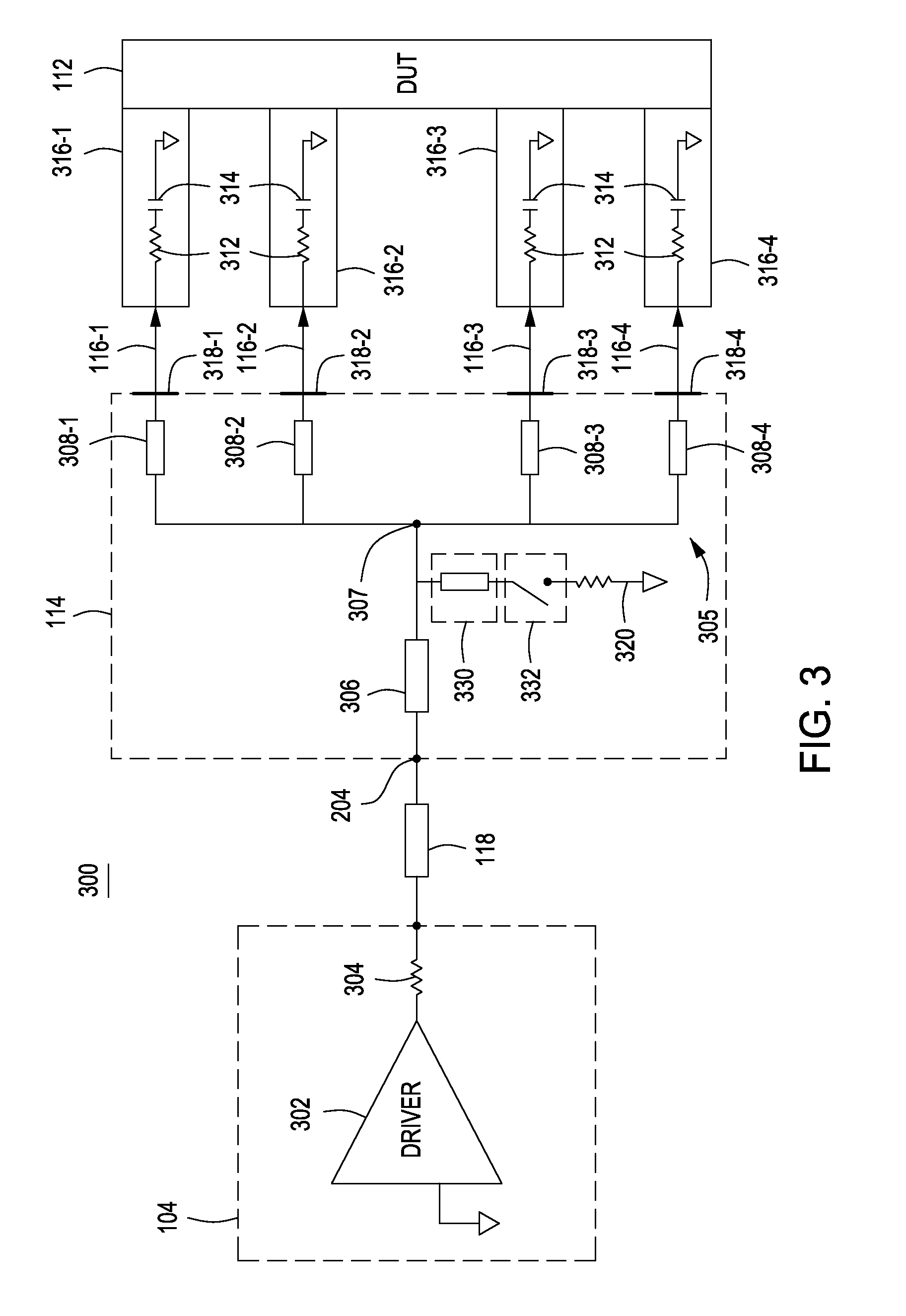
[0020]This specification describes exemplary embodiments and applications of the invention. The invention, however, is not limited to these exemplary embodiments and applications or to the manner in which the exemplary embodiments and applications operate or are described herein. Moreover, the Figures may show simplified or partial views, and the dimensions of elements in the Figures may be exaggerated or otherwise not in proportion for clarity. In addition, as the terms “on” and “attached to” are used herein, one object (e.g., a material, a layer, a substrate, etc.) can be “on” or “attached to” another object regardless of whether the one object is directly on or attached to the other object or there are one or more intervening objects between the one object and the other object. Also, directions (e.g., above, below, top, bottom, side, up, down, “x,”“y,”“z,” etc.), if provided, are relative and provided solely by way of example and for ease of illustration and discussion and not by...


PUM


Abstract

Apparatus for terminating a test signal applied to multiple semiconductor loads under test is described—for example apparatus for interfacing a test signal between a tester and a semiconductor device under test (DUT). In some examples, a probe card assembly may include at least one probe substrate each having test probes configured to contact test features of a DUT; a wiring substrate, coupled to the at least one probe substrate, having a connector configured for coupling with a source termination of a tester; a signal path formed on and/or in the wiring substrate and the at least one probe substrate, the signal path having a trace and trace stubs fanning out from the trace, an input of the trace being coupled to the connector and outputs of the trace stubs being coupled to the test probes; and a resistive termination coupled between the trace and at least one potential.

Description

BACKGROUND OF THE INVENTION[0001]1. Field of the Invention[0002]Embodiments of the present invention relate to semiconductor testing.[0003]2. Description of the Related Art[0004]Testing is an important step in the production of semiconductor devices for use. Typically, partially or fully completed semiconductor devices may be tested by bringing terminals disposed on an upper surface of a device to be tested—also referred to as a device under test (or DUT)—into contact with resilient contact elements, for example, as contained in a probe card assembly, as part of a test system. A test system controller may be coupled to the probe card assembly to send and receive test signals to and from the DUTs over a set of test channels. A test system controller with increased test channels can be a significant cost factor for a test system. Test system controllers have evolved to increase the number of channels and hence the number of devices that can be tested in parallel (sometimes referred to...

Claims


Application Information

Patent Timeline
IPC IPC(8): G01R31/02G01R31/26
CPCG01R31/31905
Inventor CHEN, GUANGMILLER, CHARLESPRITZKAU, DAVID
Owner FORMFACTOR INC
Why Eureka
Try Eureka