BBP-assisted defect detection process for SEM image
An image and defect technology used in the field of semiconductor defect detection and classification
- Summary
- Abstract
- Description
- Claims
- Application Information
AI Technical Summary
Problems solved by technology
Method used
Image

Examples
Embodiment Construction
[0031] While the claimed subject matter will be described in terms of particular embodiments, other embodiments, including those that do not provide all of the benefits and features set forth herein, are also within the scope of this disclosure. Various structural, logical, process step, and electronic changes may be made without departing from the scope of the present disclosure. Accordingly, the scope of the present disclosure is to be defined only by reference to the appended claims.
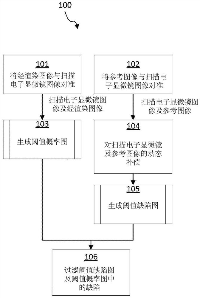
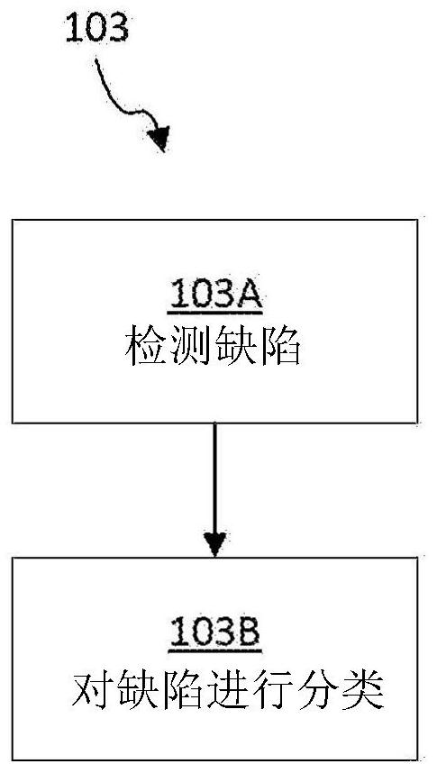
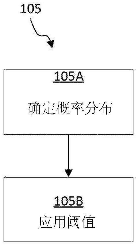
[0032] Embodiments of the present disclosure may include methods, systems, and apparatus for detecting defects on semiconductor wafers, thereby improving their accuracy in terms of true defect capture rates and disturbing point (eg, false defects) rates. Embodiments may combine reference image based detection with DL based detection. Additionally, embodiments may utilize Broadband Plasma (BBP) defect metadata to further refine detected defects. The metadata may include, among other things, ...
PUM
 Abstract
Description
Claims
Application Information
 - R&D
- Intellectual Property
- Life Sciences
- Materials
- Tech Scout
- Unparalleled Data Quality
- Higher Quality Content
- 60% Fewer Hallucinations
Browse by: Latest US Patents, China's latest patents, Technical Efficacy Thesaurus, Application Domain, Technology Topic, Popular Technical Reports.
© 2025 PatSnap. All rights reserved.Legal|Privacy policy|Modern Slavery Act Transparency Statement|Sitemap|About US| Contact US: help@patsnap.com