Magnetic clamping block and semiconductor substrate cleaning device

A cleaning device and a technology for semiconductors, which are used in the manufacture of semiconductor/solid-state devices, cleaning methods using liquids, and removal of smoke and dust. Axial rotation angle and other issues to achieve the effect of preventing damage

Active Publication Date: 2022-06-24
ZHICHENG SEMICON EQUIP TECH (KUNSHAN) CO LTD
View PDF33 Cites 5 Cited by
  • Summary
  • Abstract
  • Description
  • Claims
  • Application Information

AI Technical Summary

Problems solved by technology

For example, a substrate clamping platform disclosed in the prior art with the publication number CN111063652A, it is difficult to control the axis of the magnetic clamping block during the process of rotating the pin (or "magnetic clamping block") to clamp the wafer. The rotation angle of the magnetic clamp block is too large or too small, so that it is difficult for the magnetic clamp block to clamp the edge of the wafer, and the magnetic clamp block is easy to cause damage to the edge of the wafer during the rotation process.

Method used


Image

  • Magnetic clamping block and semiconductor substrate cleaning device
  • Magnetic clamping block and semiconductor substrate cleaning device
  • Magnetic clamping block and semiconductor substrate cleaning device

Examples


Embodiment Construction

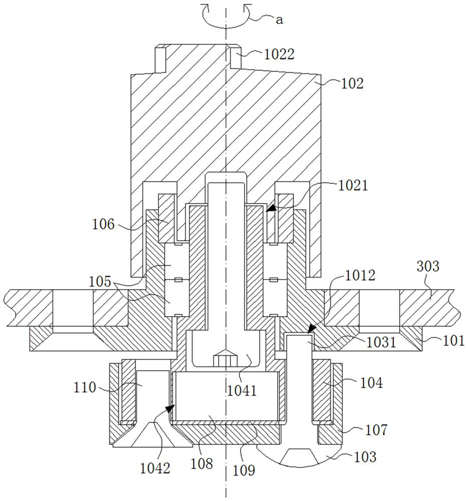
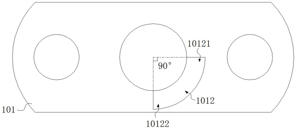
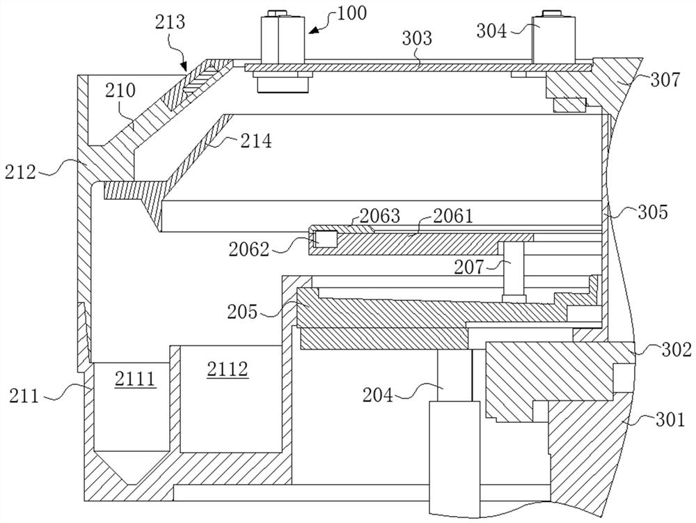
[0043] The present invention will be described in detail below with reference to the various embodiments shown in the accompanying drawings, but it should be noted that these embodiments do not limit the present invention. Equivalent transformations or substitutions all fall within the protection scope of the present invention.

[0044] It is to be understood that in this application, the terms "center", "length", "width", "thickness", "upper", "lower", "front", "rear", "left", "right" , "vertical", "horizontal", "top", "bottom", "inside", "outside", etc. indicate the orientation or positional relationship based on the orientation or positional relationship shown in the accompanying drawings, only for the convenience of describing the present technology The solution and simplified description, rather than indicating or implying that the device or element referred to must have a specific orientation, be constructed and operate in a specific orientation, should not be construed ...


PUM


Abstract

The invention provides a magnetic clamping block and a semiconductor base material cleaning device. The magnetic clamping block and the semiconductor base material cleaning device comprise a mounting base, a pivoting cylinder formed on one side of the mounting base, and a limiting assembly formed on the other side of the mounting base and coaxially arranged with the pivoting cylinder. The limiting assembly comprises a mounting part, a first magnetic block embedded in the mounting part, a mounting cover formed on the outer side of the mounting part and used for limiting axial sliding of the first magnetic block, and a limiting rod longitudinally and continuously penetrating through the mounting cover and the mounting part, and the tail end of the limiting rod extends into an arc-shaped pivoting groove formed in the mounting base. And the axial rotation angle of the pivoting cylinder relative to the mounting seat is provided through the arc-shaped pivoting groove. According to the invention, the axial rotation angle of the magnetic clamping block is accurately controlled, so that the magnetic clamping block can accurately clamp the edge of the wafer.

Description

technical field [0001] The invention relates to the technical field of semiconductor equipment, in particular to a magnetic clamping block and a semiconductor substrate cleaning device. Background technique [0002] During the processing of semiconductor substrates (taking "wafers" as an example), a cleaning device is required to clean the wafers. The semiconductor substrate cleaning device in the prior art is usually provided with a rotating mechanism for fixing and carrying wafers, and a CUP (or "splash shield") is set on the outside of the rotating mechanism, and the top of the rotating mechanism is a fixed wafer. The carrier disk (or "rotating disk") is generally adsorbed and fixed to the wafer through the negative pressure air holes set on the rotating disk, and there are also clamping blocks set on the rotating disk to achieve clamping and fixing of the wafer. . For example, a substrate clamping stage disclosed in the prior art, such as publication number CN111063652...

Claims


Application Information

Patent Timeline
Patent Type & Authority Applications(China)
IPC IPC(8): B08B3/02B08B11/02B08B15/04H01L21/67H01L21/673
CPCB08B3/022B08B3/024B08B11/02B08B15/04H01L21/67051H01L21/67333
Inventor 蔡超赵天翔刘国强
Owner ZHICHENG SEMICON EQUIP TECH (KUNSHAN) CO LTD
Why Eureka
Try Eureka