Manufacturing method of PTH half hole of PCB

A technology of PCB board and manufacturing method, which is applied in the field of PTH semi-hole manufacturing, can solve problems such as bridge junction short circuit, copper skin defect, virtual soldering, etc., and achieve the effect of precise size control

Pending Publication Date: 2022-06-24
科惠白井(佛冈)电路有限公司
View PDF7 Cites 1 Cited by
  • Summary
  • Abstract
  • Description
  • Claims
  • Application Information

AI Technical Summary

Problems solved by technology

[0002] In the PTH half-hole manufacturing process of the existing PCB board, after the PTH half-hole is formed, the hole wall is prone to residual burrs and copper wires on the hole wall. If the burrs are not removed cleanly, it may even cause a short circuit
A common method is to drill the PTH half hole twice, then dry the film a second time, and finally etch again to remove the burr. This method needs to add three additional processing steps in the PTH half hole process, which improves the processing. time and cost; and it is easy to cause side erosion during etching to cause the copper defect of the PTH half-hole wall again, resulting in weak solder joints and virtual soldering in the subsequent welding process

Method used


Image

  • Manufacturing method of PTH half hole of PCB
  • Manufacturing method of PTH half hole of PCB
  • Manufacturing method of PTH half hole of PCB

Examples


Embodiment Construction

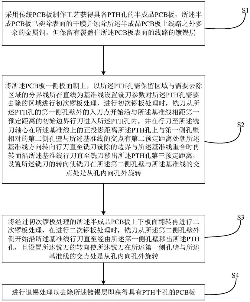
[0020] The present application will be further described in detail below with reference to the accompanying drawings and specific embodiments. It should be understood that the following exemplary embodiments and descriptions are only used to explain the present invention, but not to limit the present invention, and, in the case of no conflict, the embodiments in the present application and the features in the embodiments can be combined with each other .

[0021] like Figure 1-Figure 3 As shown, an optional embodiment of the present invention provides a method for manufacturing a PTH half hole of a PCB board, comprising the following steps:

[0022] S1: A semi-finished PCB board with PTH hole 1 is obtained by using the traditional PCB board manufacturing process. The semi-finished PCB board has been removed from the surface dry film and etched away excess metal copper except for the lines on the semi-finished PCB board, but retained There is a tinned layer covering the line...


PUM


Abstract

The embodiment of the invention provides a method for manufacturing a PTH half hole of a PCB, and the method comprises the steps: taking a semi-finished PCB, setting milling cutter parameters by taking a boundary between a PTH hole reservation region and a PTH hole removal region as a reference line, carrying out the primary milling of a PTH hole, and enabling a cutter entering point of a milling cutter located on a first side hole wall of the PTH hole to be away from the reference line by a first preset distance, moving the cutter along the datum line until the orthographic projection of the axis of the milling cutter on the datum line is a second preset distance away from the intersection point of a second side hole wall opposite to the first side hole wall on the PTH hole and the datum line, rotating the cutter to move along the datum line until the milling cutter moves out of the PTH hole by a third preset distance, and turning over the upper and lower plate surfaces to carry out secondary milling treatment on the PCB, and the milling cutter moves from the outer side of the second side hole wall along the datum line until the milling cutter moves out of the PTH through the first side hole wall, and the milling cutter rotates from the inside to the outside of the hole at the first side hole wall and the second side hole wall. According to the embodiment of the invention, the high-quality PTH half hole is obtained by scientifically setting the distance position of the cutter feeding point relative to the reference line and the rotation direction of the milling cutter.

Description

technical field [0001] Embodiments of the present invention relate to the technical field of PCB board processing, and in particular, to a method for manufacturing a PTH half hole of a PCB board. Background technique [0002] In the PTH half-hole manufacturing process of the existing PCB board, after the PTH half-hole is formed, the hole wall is prone to the phenomenon of residual copper wire with burrs on the hole wall. The common method is to drill the PTH half hole for a second time, then perform a second dry film film, and finally remove the burr by etching again. This method requires three additional processing steps in the PTH half hole process, which improves the processing. In addition, the side etching is easy to cause the copper skin defect of the PTH half-hole hole wall again during etching, which leads to the phenomenon of weak solder joints and virtual soldering in the subsequent welding process. SUMMARY OF THE INVENTION [0003] The technical problem to be s...

Claims


Application Information

Patent Timeline
Patent Type & Authority Applications(China)
IPC IPC(8): H05K3/00
CPCH05K3/0055H05K3/0047
Inventor 罗家亮梅正中欧阳润胜
Owner 科惠白井(佛冈)电路有限公司
Why Eureka
Try Eureka