Chip system integration method and device and computer readable storage medium

A chip system and integration method technology, applied in CAD circuit design and other directions, can solve problems such as low integration efficiency, achieve accurate and reasonable classification, storage, and avoid low processing efficiency.

Pending Publication Date: 2022-07-01
比科奇微电子(杭州)有限公司
View PDF0 Cites 2 Cited by
  • Summary
  • Abstract
  • Description
  • Claims
  • Application Information

AI Technical Summary

Problems solved by technology

[0005] Embodiments of the present invention provide a chip system integration method, device, and computer-readable storage medium to

Method used


Image

  • Chip system integration method and device and computer readable storage medium
  • Chip system integration method and device and computer readable storage medium
  • Chip system integration method and device and computer readable storage medium

Examples


Embodiment 1

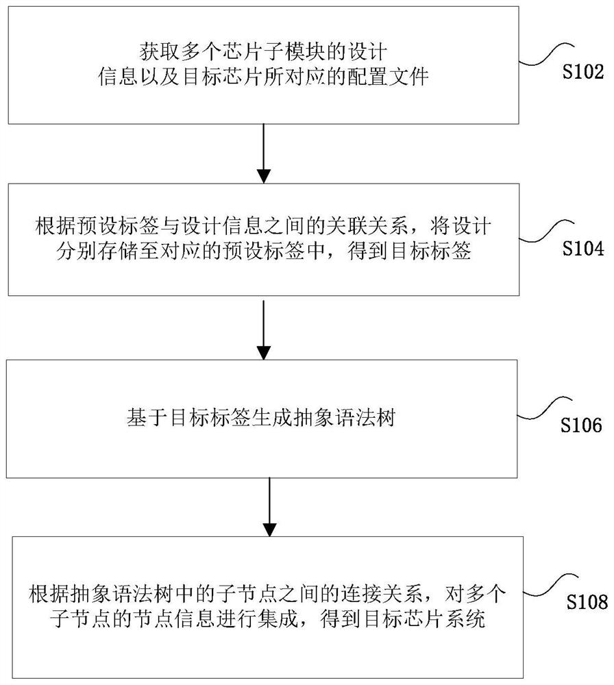
[0030]According to an embodiment of the present invention, a method embodiment of a method for integrating a chip system is provided. It should be noted that the steps shown in the flowchart of the accompanying drawings may be executed in a computer system such as a set of computer-executable instructions, Also, although a logical order is shown in the flowcharts, in some cases the steps shown or described may be performed in an order different from that herein.

[0031] In addition, it should also be noted that an electronic device can be used as the execution body of the method for integrating the chip system in the embodiment of the present invention.

[0032] figure 1 is a flowchart of an optional chip system integration method according to an embodiment of the present invention, such as figure 1 As shown, the method includes the following steps:

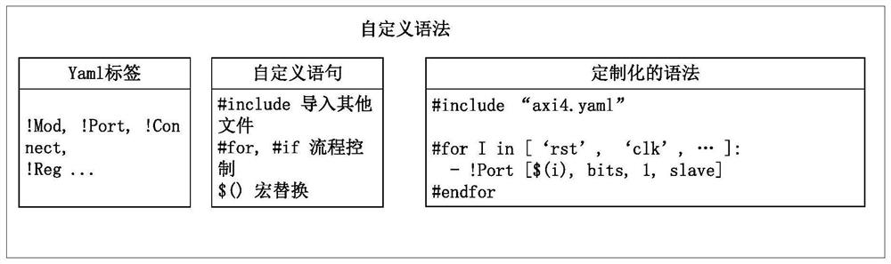
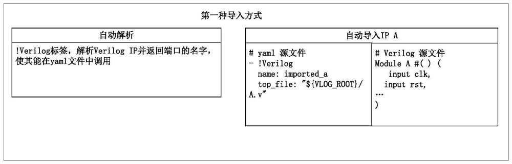
[0033] Step S102 , acquiring design information of a plurality of chip sub-modules and configuration files corresponding to ...

Embodiment 2

[0091] According to another aspect of the embodiments of the present invention, an integrated device of a chip system is also provided, wherein, Figure 7 It is a schematic diagram of an integrated device of a chip system according to an embodiment of the present invention. like Figure 7 As shown, the apparatus includes: an acquisition module 701 , a storage module 702 , a generation module 703 and an integration module 704 .

[0092] The acquisition module 701 is used for acquiring design information of multiple chip sub-modules and configuration files corresponding to the target chip, wherein the configuration files at least include preset tags for storing design information, and the multiple chip sub-modules are used for Integrate the target chip; the storage module 702 is used to store the design information in the corresponding preset labels according to the association relationship between the preset labels and the design information, so as to obtain a plurality of tar...

Embodiment 3

[0101] Optionally, according to another aspect of the embodiments of the present invention, there is also provided a computer-readable storage medium, where a computer program is stored in the computer-readable storage medium, wherein the computer program is configured to execute the above embodiments when running 1. The integration method of the system-on-a-chip.


PUM


Abstract

The invention discloses a chip system integration method and device and a computer readable storage medium. The method comprises the steps that design information of a plurality of chip sub-modules and a configuration file corresponding to a target chip are obtained, the configuration file at least comprises a preset label used for storing the design information, and the chip sub-modules are used for integrating the target chip; according to the incidence relation between the preset labels and the design information, the design information is stored in the corresponding preset labels, and target labels are obtained; an abstract syntax tree is generated based on the target labels, the abstract syntax tree is composed of a plurality of child nodes, and each child node corresponds to one target label; and according to a connection relationship among the child nodes in the abstract syntax tree, integrating node information of the plurality of child nodes to obtain a target chip system. The technical problem that in the prior art, the integration efficiency is low when an integrated chip system is manually configured is solved.

Description

technical field [0001] The present invention relates to the field of chip design, and in particular, to an integrated method, device and computer-readable storage medium of a chip system. Background technique [0002] Ultra-large-scale SoC (System on chip, system-on-chip) integrated circuit design is usually designed using multiple existing chip sub-modules, and these chip sub-modules have their own IP (Intellectual Property, intellectual property) design information, so as to operate Personnel can integrate existing IP design information to generate complex chip systems. [0003] However, in the prior art, an operator is usually required to parse and process the existing IP design information first, and then manually configure and integrate the processed IP design information. This process requires a lot of time, and Since the problem of configuration errors is prone to occur in the manual configuration process, the integration efficiency of the chip system is low. [000...

Claims


Application Information

Patent Timeline
IPC IPC(8): G06F30/32
CPCG06F30/32
Inventor 孙超李旸李申煜沈钲蒋颖波
Owner 比科奇微电子(杭州)有限公司
Why Eureka
Try Eureka