Wafer pre-alignment device and wafer pre-alignment method

A pre-alignment, wafer technology, applied in the direction of semiconductor/solid-state device parts, semiconductor devices, electrical components, etc., can solve the failure to meet the requirements of wafer pre-alignment accuracy, pre-alignment failure, and damage to wafer geometric features and other issues to achieve the effect of meeting the alignment requirements of wafer lithography and improving precision

Pending Publication Date: 2022-07-01
SHANGHAI MICRO ELECTRONICS EQUIP (GRP) CO LTD
View PDF0 Cites 9 Cited by
  • Summary
  • Abstract
  • Description
  • Claims
  • Application Information

AI Technical Summary

Problems solved by technology

However, in the following working conditions, conventional pre-alignment methods cannot meet the requirements of wafer pre-alignment accuracy
[0003] (1) There are many kinds of bonding sheets on the market, mechanical bonding is adopted, or the previous process is poor, resulting in horizontal offset and uncertain angular deviation between the bottom carrier and the upper bonding sheet
After the pre-alignment equipment based on the geometric characteristics of the wafer completes the positioning of the wafer, the mark on the wafer cannot enter the alignment field of view, and the alignment system cannot find the mark according to the nominal position of the mark, which eventually leads to the failure of alignment;
[0004] (2) The geometric features of the wafer (such as outer circle or notch or flat edge) are damaged, resulting in pre-alignment failure

Method used


Image

  • Wafer pre-alignment device and wafer pre-alignment method
  • Wafer pre-alignment device and wafer pre-alignment method
  • Wafer pre-alignment device and wafer pre-alignment method

Examples


Embodiment Construction

[0104] The present invention will be further described in detail below in conjunction with the accompanying drawings and embodiments. It should be understood that the specific embodiments described herein are only used to explain the present invention, but not to limit the present invention. In addition, it should be noted that, for the convenience of description, the drawings only show some but not all structures related to the present invention.

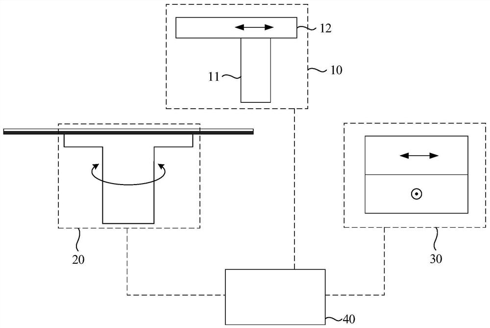
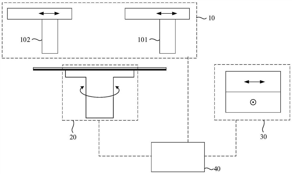
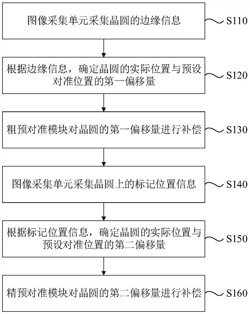
[0105] figure 1 It is a schematic structural diagram of a wafer pre-alignment device provided by an embodiment of the present invention, refer to figure 1 , the wafer pre-alignment device includes: an image acquisition module 10 for respectively collecting edge information of the wafer and mark position information on the wafer; a data processing module 40 for determining the actual position of the wafer according to the edge information The first offset from the preset alignment position, according to the mark position informati...


PUM


Abstract

The embodiment of the invention discloses a wafer pre-alignment device and a wafer pre-alignment method. The device comprises an image acquisition module which comprises an image acquisition unit and a camera position switching mechanism and is used for respectively acquiring edge information of a wafer and position information marked on the wafer; the data processing module is used for respectively determining a first offset and a second offset between the actual position of the wafer and a preset alignment position according to the edge information and the mark position information; the coarse pre-alignment module is used for compensating the first offset of the wafer; and the fine pre-alignment module is used for compensating the second offset of the wafer. The problem that an existing alignment device is large in pre-alignment precision deviation is solved, the pre-alignment precision can be improved, the device can be suitable for pre-alignment of various bonding pieces, and the follow-up wafer photoetching alignment requirement is met.

Description

technical field [0001] Embodiments of the present invention relate to the technical field of integrated circuit manufacturing, and in particular, to a wafer pre-alignment device and a wafer pre-alignment method. Background technique [0002] Wafer pre-alignment is an important module of the transfer subsystem. The transfer robot takes the wafer from the wafer storage (FOUP or cassette), and after the wafer is centered and oriented by the wafer pre-alignment equipment, it is loaded by the robot to the wafer. The workpiece table is then moved to the alignment station for alignment. It is required that after the wafer is initially positioned by the pre-alignment equipment, the mark on the wafer can enter the alignment field of view. Due to the high positional accuracy of wafer marks relative to wafer geometry, conventional wafer pre-alignment is based on wafer outer circle geometry to achieve wafer centering, such as edge notch or flat edge to achieve wafer centering. Circle ...

Claims


Application Information

Patent Timeline
Patent Type & Authority Applications(China)
IPC IPC(8): H01L21/68H01L23/544
CPCH01L21/681H01L23/544H01L2223/54426
Inventor 王刚杨思雨付红艳郎新科刘浩
Owner SHANGHAI MICRO ELECTRONICS EQUIP (GRP) CO LTD
Why Eureka
Try Eureka