Check patentability & draft patents in minutes with Patsnap Eureka AI!

Semiconductor memory device

A memory and device technology, applied in the direction of semiconductor devices, electric solid state devices, electrical components, etc., can solve the problems of high delay in process change programming speed, etc.

Pending Publication Date: 2022-07-01
GLOBALFOUNDRIES SINGAPORE PTE LTD
View PDF0 Cites 0 Cited by
  • Summary
  • Abstract
  • Description
  • Claims
  • Application Information

AI Technical Summary

Problems solved by technology

[0003] However, memory devices can present multiple challenges such as sensitivity to process variations and high latency in programming speed

Method used


Image

  • Semiconductor memory device
  • Semiconductor memory device
  • Semiconductor memory device

Examples


Embodiment Construction

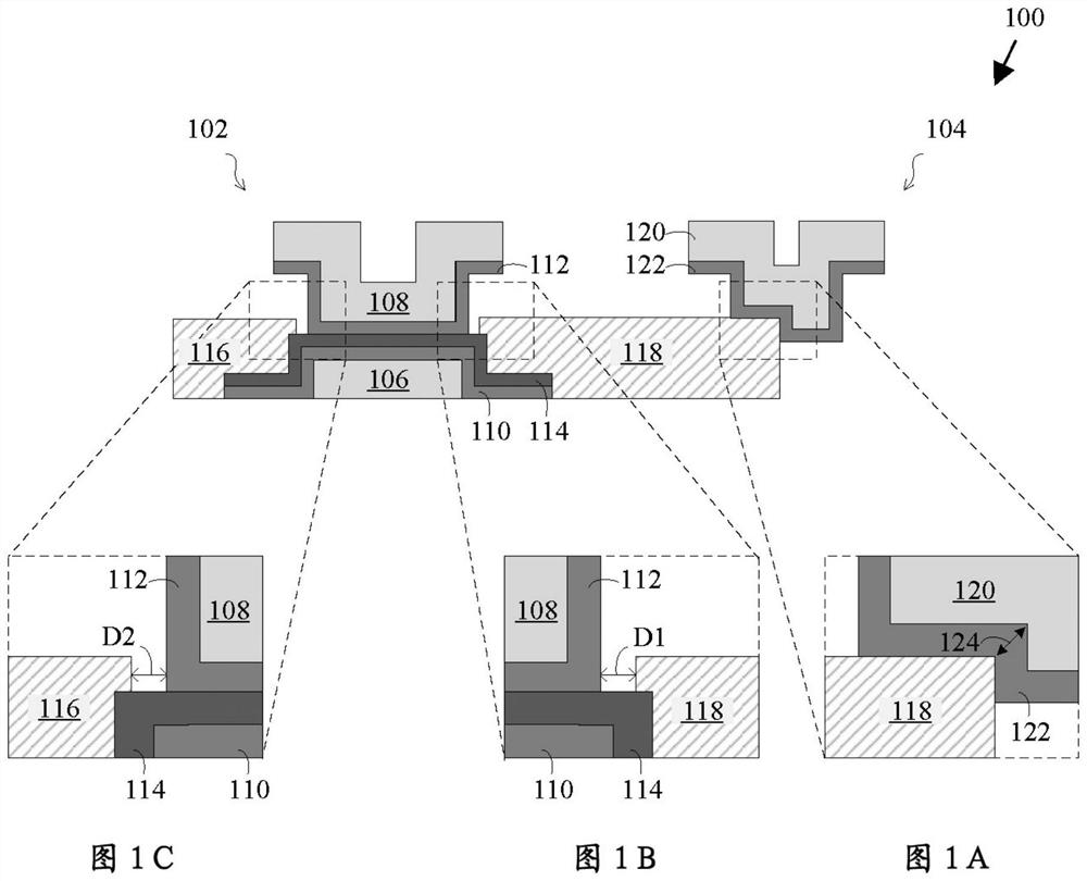
[0019] The present disclosure relates generally to semiconductor devices, and more particularly to semiconductor memory devices and methods of forming the same. The semiconductor memory device improves device performance with a smaller footprint.

[0020] Resistive random access memory (RRAM) cells typically include a pair of memory electrodes and a switching layer interposed between the pair of memory electrodes. The switching layer of an RRAM cell is usually insulating.

[0021] RRAM cells operate by switching between states based on the resistance of the switching layer. For example, when a sufficiently high voltage difference is applied between the two memory electrodes, a dielectric breakdown event may occur and one or more conducting filaments may form within the switching layer. The switching layer becomes conductive as one or more conductive filaments are formed. By applying a low enough voltage difference between the two memory electrodes to break the one or more c...


PUM


Abstract

Embodiments herein relate to semiconductor memory devices and methods of forming the same. A semiconductor memory device is provided. The semiconductor memory device includes a dual gate transistor and a memory cell. The memory cell is adjacent to the dual-gate transistor, wherein the memory cell and the dual-gate transistor share a common electrode.

Description

technical field [0001] The present disclosure relates generally to semiconductor devices, and more particularly to semiconductor memory devices and methods of forming the same. Background technique [0002] Semiconductor memory devices can generally be classified into volatile memory devices and non-volatile memory (NVM) devices. A resistive random access memory (RRAM) device is a type of non-volatile memory (NVM) device used in advanced computing systems, such as for processing in memory (PIM) using binary neural network (BNN) based techniques Applications and Machine Learning (ML) applications. RRAM devices are suitable for such applications because they can provide a high-density architecture with high parallel programming speed and low power consumption. [0003] However, memory devices can present multiple challenges, such as sensitivity to process variations and high latency for programming speed. High-density memory device arrays are needed to improve the accuracy ...

Claims


Application Information

Patent Timeline
IPC IPC(8): H01L29/417H01L29/423H01L45/00H01L27/24
CPCH01L29/42356H01L29/41725H10B63/30H10N70/841H01L29/66969H01L29/7869H01L29/78696H01L29/78648H01L29/66765H01L29/78669H10N70/011
Inventor 陈学深蔡新树卓荣发
Owner GLOBALFOUNDRIES SINGAPORE PTE LTD
Features
  • R&D
  • Intellectual Property
  • Life Sciences
  • Materials
  • Tech Scout
  • Unparalleled Data Quality
  • Higher Quality Content
  • 60% Fewer Hallucinations
Learn More