Deep learning wafer welding spot detection method based on improved YOLOV5

A technology of solder joint detection and deep learning, applied in the field of target detection, to improve the accuracy of target detection, improve the ability of network feature extraction, and reduce the effect of information loss

Pending Publication Date: 2022-07-08
GUANGXI NORMAL UNIV
View PDF0 Cites 1 Cited by
  • Summary
  • Abstract
  • Description
  • Claims
  • Application Information

AI Technical Summary

Problems solved by technology

However, due to the particularity of the detection target, the YOLOV5 algorithm still has a certain room for optimization for the wafer solder joint detection task.

Method used


Image

  • Deep learning wafer welding spot detection method based on improved YOLOV5
  • Deep learning wafer welding spot detection method based on improved YOLOV5
  • Deep learning wafer welding spot detection method based on improved YOLOV5

Examples


Embodiment

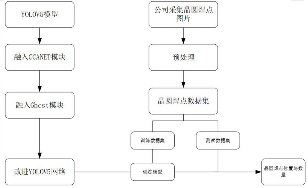
[0053] refer to figure 1 , a deep learning wafer solder joint detection method based on improved YOLOV5, comprising the following steps:

[0054] 1) Making a data set of wafer solder joints: collect images of wafer solder joints, preprocess the collected wafer solder joint images to improve the number of samples and picture quality of the data set, and then mark the data set to meet the needs of The aligned solder joints and the solder joints that do not need to be aligned are marked with rectangles. The solder joints that need to be aligned are named Rig holes, and the solder joints that do not need to be aligned are named Wro holes, and finally a 1464 wafer solder joint images are produced. Wafer solder joint data set, and divide the data set into training set and validation set with a ratio of 9:1;

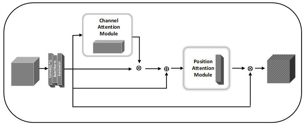
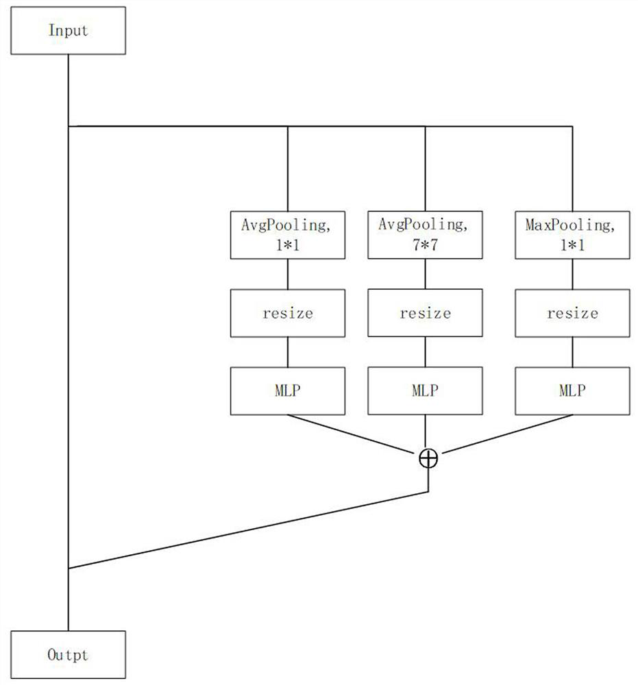
[0055] 2) Construct the attention mechanism module CCANET: The attention mechanism module CCANET is as follows figure 2 shown, including:

[0056] 2.1) Firstly, a filter mo...


PUM


Abstract

The invention discloses a deep learning wafer welding spot detection method based on improved YOLOV5. The method comprises the following steps: 1) making a wafer welding spot data set; the method comprises the following steps of (1) constructing an attention mechanism module CCANET, (2) constructing a YOLOV5 network integrated with an attention mechanism, (4) introducing a Ghost module, and (5) training and improving the YOLOV5 network.According to the method, under the condition that fewer network parameters are used, the wafer welding spot detection precision is improved, and under the same condition, more wafer welding spots can be detected, and shielded wafer welding spots can also be detected.

Description

technical field [0001] The invention relates to the technical field of target detection, in particular to a deep learning wafer solder joint detection method based on improved YOLOV5. Background technique [0002] With the increasing complexity of chips and more and more modules and functions inside the chip, how to effectively test wafers is considered more and more in the entire chip design. At the same time, wafer testing is one of the most important statistical methods for chip yield. Improving chip yield can greatly reduce chip production losses in industrial production and improve chip production efficiency. Therefore, wafer testing has a very important strategic significance in the entire chip fabrication. [0003] Wafer test is to perform needle test on each die on the wafer, use the probe on the inspection head to contact the solder joint, and then measure the capacity and other properties of the wafer through electrical testing, in which the contact between the pr...

Claims


Application Information

Patent Timeline
Patent Type & Authority Applications(China)
IPC IPC(8): G06T7/90G06T7/11G06T7/00G06N3/04G06K9/62G06V10/774G06V10/82
CPCG06T7/0004G06T7/11G06T7/90G06T2207/20132G06T2207/30148G06N3/045G06F18/214Y02P90/30
Inventor 许江杰邹艳丽谭宇飞余自淳
Owner GUANGXI NORMAL UNIV
Why Eureka
Try Eureka