
Display substrate, manufacturing method thereof, display panel and display device

A display substrate and display panel technology, which is applied in semiconductor/solid-state device manufacturing, electrical components, electric solid-state devices, etc., can solve the problems of reducing display power consumption, failing to meet the requirements of high color gamut, and achieving Improve the effect of color gamut range, luminous efficiency and high brightness

Pending Publication Date: 2022-07-08
BOE TECH GRP CO LTD
View PDF0 Cites 2 Cited by
  • Summary
  • Abstract
  • Description
  • Claims
  • Application Information

AI Technical Summary

Problems solved by technology

[0003] However, currently existing display substrates cannot meet the requirements of high color gamut, and cannot meet the requirements of reducing display power consumption while displaying high color gamut

Method used


Image

  • Display substrate, manufacturing method thereof, display panel and display device
  • Display substrate, manufacturing method thereof, display panel and display device
  • Display substrate, manufacturing method thereof, display panel and display device

Examples


Embodiment Construction

[0051] Example embodiments will now be described more fully with reference to the accompanying drawings. Example embodiments, however, can be embodied in various forms and should not be construed as limited to the embodiments set forth herein; rather, these embodiments are provided so that this disclosure will be thorough and complete, and will fully convey the concept of example embodiments to those skilled in the art. The same reference numerals in the drawings denote the same or similar structures, and thus their detailed descriptions will be omitted. Furthermore, the drawings are merely schematic illustrations of the present disclosure and are not necessarily drawn to scale.

[0052] Although relative terms such as "upper" and "lower" are used in this specification to describe the relative relationship of one component of an icon to another component, these terms are used in this specification only for convenience, such as according to the direction of the example descri...


PUM


Abstract

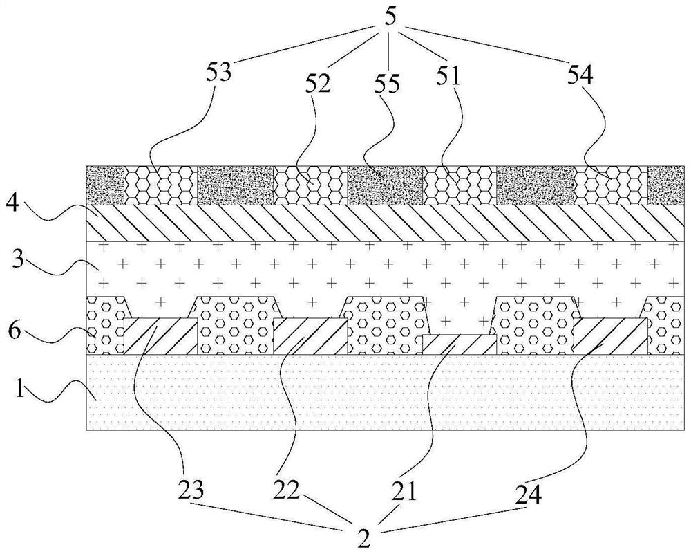
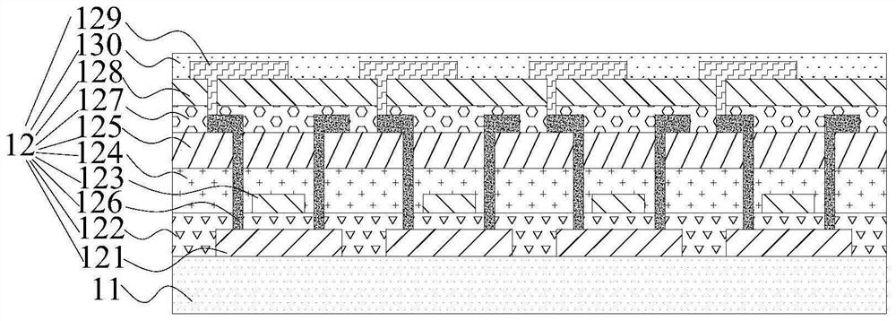
The invention provides a display substrate, a manufacturing method of the display substrate, a display panel and a display device. The first electrode layer is arranged on one side of the driving backboard and at least comprises a plurality of electrode blocks arranged in an array mode, the electrode blocks comprise the first electrode blocks and the second electrode blocks, and the thickness of the first electrode blocks is smaller than that of the second electrode blocks; the light-emitting material layer covers the electrode block, and the light-emitting material layer is of a continuous whole-layer structure; a second electrode layer covering the light emitting material layer; the color film layer is arranged on the side, away from the driving backboard, of the second electrode layer and comprises a green first light filtering area and a red second light filtering area, and the orthographic projection of the first light filtering area on the driving backboard is at least partially overlapped with the orthographic projection of the first electrode block on the driving backboard; and the orthographic projection of the second filtering area on the driving back plate is at least partially overlapped with the orthographic projection of the second electrode block on the driving back plate. According to the display substrate, the display power consumption can be reduced while high-color-gamut display is achieved.

Description

technical field [0001] The present disclosure relates to the field of display technology, and in particular, to a display substrate and a manufacturing method thereof, a display panel and a display device. Background technique [0002] In the art, in order for the display substrate to meet the high display color gamut requirements, greener green light and redder red light that the display substrate can emit is required. [0003] However, the current existing display substrates cannot meet the requirements of high color gamut, and also cannot meet the requirements of reducing display power consumption while displaying high color gamut. [0004] It should be noted that the information disclosed in the above Background section is only for enhancement of understanding of the background of the present disclosure, and therefore may contain information that does not form the prior art that is already known to a person of ordinary skill in the art. SUMMARY OF THE INVENTION [000...

Claims


Application Information

Patent Timeline
Patent Type & Authority Applications(China)
IPC IPC(8): H01L51/52H01L27/32H01L21/77
CPCH10K59/351H10K59/38H10K59/12H10K50/813H10K59/1201
Inventor 王琳琳尤娟娟
Owner BOE TECH GRP CO LTD
Learn More