TM0-TE1 optical mode converter based on double-layer curve edge waveguide structure and optical device

A technology of TM0-TE1 and waveguide structure, which is applied in the field of integrated photonics, can solve the problems that it is difficult to take into account the compact size of the device and high conversion efficiency at the same time, achieve high mode conversion efficiency, ensure smoothness, and ensure the effect of manufacturability

Active Publication Date: 2022-07-15
ZHEJIANG LAB
View PDF8 Cites 1 Cited by
  • Summary
  • Abstract
  • Description
  • Claims
  • Application Information

AI Technical Summary

Problems solved by technology

The traditional TM0-TE1 mode converter based on the double-layer linear graded waveguide structure usually needs a long size to complete the sm

Method used


Image

  • TM0-TE1 optical mode converter based on double-layer curve edge waveguide structure and optical device
  • TM0-TE1 optical mode converter based on double-layer curve edge waveguide structure and optical device
  • TM0-TE1 optical mode converter based on double-layer curve edge waveguide structure and optical device

Examples


Example Embodiment

[0033] Example 1:

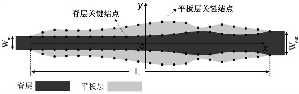
[0034] see Figure 4-Figure 5 , the material of the ridge layer and the plate layer is set to silicon, the periphery of the waveguide is set to silicon dioxide, the thickness H2 of the plate layer is set to 90nm, and the height H1 of the top of the ridge layer relative to the bottom of the plate layer is set to 220nm.

[0035] Introduce the wave into the port width W in Fixed at 440nm, the waveguide exit width W out It was fixed at 800 nm, and the device length L was fixed at 8 μm. The device has an axisymmetric structure along the light propagation direction. We set 21 equally spaced key nodes for each edge of the ridge-layer and slab-layer waveguides, and connected them through quadratic spline interpolation.

[0036] We fixed the position of the first node, and optimized the ordinates of the 38 free nodes in the middle using the adjoint optimization method based on 3-dimensional finite difference time domain (FDTD). The optimization goal was to maxim...

Example Embodiment

[0038] Embodiment 2:

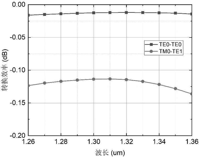
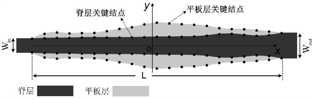
[0039] see Figure 6-Figure 7 , and then the thickness of the slab layer H 2 Change to 70nm, keep other materials and parameters unchanged, reuse the concomitant optimization method based on 3-dimensional finite difference time domain (FDTD) to optimize the ordinates of the 38 free nodes in the middle. The final optimized mode converter structure is as follows Image 6 As shown, it has a smooth waveguide edge shape and is easy to fabricate. The conversion efficiency obtained by 3D FDTD simulation is as follows Figure 7 As shown, it still has very high TM0-TE1 mode conversion efficiency and TE0-TE0 mode transmittance.


PUM


Abstract

The invention provides a TM0-TE1 optical mode converter based on a double-layer curve edge waveguide structure and an optical device, the mode converter is provided with a double-layer waveguide structure, each layer of waveguide comprises a plurality of key nodes of which the positions can be optimized, and the specific shape of the waveguide edge is determined through a quadratic or cubic spline interpolation method. The mode converter can convert a transverse magnetic fundamental mode, namely a TM0 mode, of an input waveguide into a first-order transverse electric mode, namely a TE1 mode, and meanwhile, the input transverse electric fundamental mode, namely the TE0 mode, is not changed. Compared with a traditional TM0-TE1 mode converter based on a double-layer linear gradient waveguide structure, the TM0-TE1 mode converter has the advantages that higher mode conversion efficiency can be obtained by optimizing denser key node parameters in a more compact size, meanwhile, the smoothness of the edge of the waveguide can be strictly guaranteed, and it is guaranteed that the technology can be used for preparing the TM0-TE1 mode converter.

Description

technical field [0001] The invention relates to the technical field of integrated photonics, in particular to a TM0-TE1 optical mode converter and an optical device based on a double-layer curved edge waveguide structure. Background technique [0002] In the field of integrated optics, most of the integrated photonic devices have special requirements on the polarization state of incident light, for example, they only work normally when the polarization state of the transverse electric mode (TE) is incident. The polarization diversity receiving scheme based on the on-chip polarization rotation beam splitter can solve this problem well. The polarization rotation beam splitter can divide the transverse electric mode (TE) and transverse magnetic mode (TM) components of the incident light into two paths, and the TM components are converted to TE components. The polarization rotation beam splitter is generally composed of a TM0-TE1 optical mode converter and a TE0 / TE1 mode splitt...

Claims


Application Information

Patent Timeline
IPC IPC(8): G02B6/10G02B6/14
CPCG02B6/10G02B6/14G02B2006/12152G02B2006/12097G02B2006/12061
Inventor 阮小可储涛
Owner ZHEJIANG LAB
Why Eureka
Try Eureka