Optical device production, processing and packaging device and packaging method thereof

A technology for packaging devices and optical devices, applied in the coupling of optical waveguides, etc., can solve the problems of increased labor intensity, inconvenient clamping and packaging of anti-drop nets, and easy sliding

Inactive Publication Date: 2022-07-15
深圳市兆捷科技有限公司
View PDF1 Cites 0 Cited by
  • Summary
  • Abstract
  • Description
  • Claims
  • Application Information

AI Technical Summary

Problems solved by technology

[0004] The existing packaging device is too simple. On the one hand, it is inconvenient for the device to realize automatic packaging. When packaging, manual cooperation is required to complete the packaging work, which increases labor intensity. The surface is hollowed out, and when clamping, the clamping surface is limited, it is not easy to be easily clamped, and it is easy to cause sliding, so it is not convenient to clamp and package the anti-drop net stably. For this reason, we propose a production, processing and packaging device for optical devices and its encapsulation method

Method used


Image

  • Optical device production, processing and packaging device and packaging method thereof
  • Optical device production, processing and packaging device and packaging method thereof
  • Optical device production, processing and packaging device and packaging method thereof

Examples


Embodiment Construction

[0037] The following description serves to disclose the invention to enable those skilled in the art to practice the invention. The preferred embodiments described below are given by way of example only, and other obvious modifications will occur to those skilled in the art.

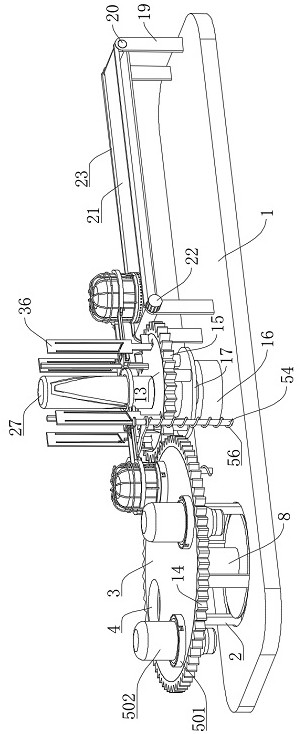
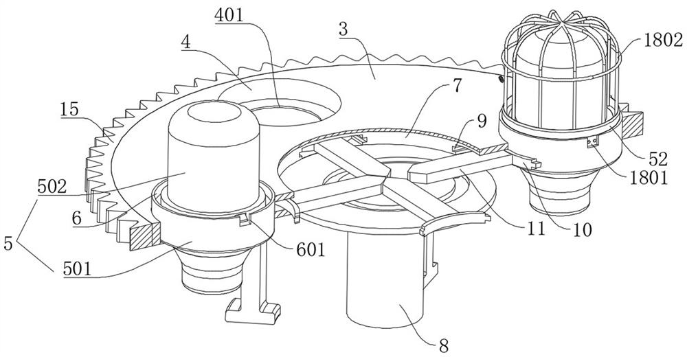
[0038] like Figure 2 to Figure 12 The shown optical device production, processing and packaging device includes a bottom plate 1 and a second circular plate 13. The top of the bottom plate 1 is slidably connected with four sliders 2, and the tops of the four sliders 2 are jointly and fixedly connected with a first circular plate. 3, is characterized in that, the top of the first circular plate 3 is provided with four first placement slots 4 in a circular array, the inner bottom of the first placement slot 4 is provided with a first through port 401, and the first placement slot 4 is inserted with Explosion-proof lamp 5. The explosion-proof lamp 5 is composed of a lamp holder 501 and a bulb 502 that are...


PUM


Abstract

The invention relates to the technical field of optical device packaging, in particular to an optical device producing, processing and packaging device and a packaging method thereof.The optical device producing, processing and packaging device comprises a bottom plate and a second circular plate, the top of the bottom plate is slidably connected with four sliding blocks, and the tops of the four sliding blocks are jointly and fixedly connected with a first circular plate; four first placement grooves are formed in the top of the first circular plate in a circumferential array mode, first through openings are formed in the bottoms in the first placement grooves, explosion-proof lamps are inserted into the first placement grooves and are composed of lamp holders and bulbs which are fixedly connected with one another, first annular grooves are formed in the tops of the lamp holders, and first through openings are formed in the bottoms in the first placement grooves; second through openings are symmetrically formed in the side wall of the first annular groove. The reciprocating mechanism drives the mounting block to move downwards, the mounting block moving downwards close to the packaging station can insert the anti-falling net cover into the first annular groove in the top of the lamp holder through the clamping mechanism, and therefore one-time packaging of the explosion-proof lamp and the anti-falling net cover is completed, manual packaging is not needed in the whole process, and more automation is achieved.

Description

technical field [0001] The invention relates to the field of optical device packaging, in particular to an optical device production and processing packaging device and a packaging method thereof. Background technique [0002] Optical devices are divided into active devices and passive devices. Optical active devices are optoelectronic devices that can convert electrical signals into optical signals or convert optical signals into electrical signals that require additional energy to drive work in optical communication systems. the heart of the system. Optical passive devices are optoelectronic devices that do not require external energy to drive work. For example, some semiconductor light-emitting diodes, explosion-proof lamps, fiber optic couplers, etc. [0003] The prior art discloses some patent documents on optical device packaging. The Chinese patent application number 202011069984.0 discloses a patent for an optical device production, processing and packaging device,...

Claims


Application Information

Patent Timeline
Patent Type & Authority Applications(China)
IPC IPC(8): G02B6/42
CPCG02B6/4251
Inventor 余学刚吴剑锋孙成成
Owner 深圳市兆捷科技有限公司
Why Eureka
Try Eureka