Supercharge Your Innovation With Domain-Expert AI Agents!

Deviation detection method and device for mechanical arm of semiconductor equipment

A deviation detection and robotic arm technology, applied in manipulators, manufacturing tools, etc., can solve problems such as robotic arm collision, wafer transfer failure, and inability to accurately estimate robotic arm maintenance timing, so as to avoid production accidents and achieve efficient and timely detection. , Accurately estimate the effect of maintenance timing

Active Publication Date: 2022-07-29
江苏邑文微电子科技有限公司 +1
View PDF8 Cites 0 Cited by
  • Summary
  • Abstract
  • Description
  • Claims
  • Application Information

AI Technical Summary

Problems solved by technology

Based on this, semiconductor process equipment has very high requirements for the movement accuracy of the robotic arm. If the movement accuracy of the robotic arm deviates, it will cause accidents such as wafer transfer failure and robotic arm hitting other equipment components.
However, the ultra-high temperature, vacuum or ultra-high pressure working environment in the semiconductor process equipment is very easy to damage the parts of the robot arm, which will cause the robot arm to deviate during transmission
[0003] The existing technology usually uses professional testing equipment to manually detect the deviation of the robotic arm during the regular maintenance of semiconductor process equipment. Deviations cannot be dealt with in time
At the same time, due to the gradual accumulation of the deviation of the mechanical arm, the existing technology cannot accurately predict the maintenance timing of the mechanical arm, which in turn leads to frequent production accidents caused by the deviation of the mechanical arm

Method used


Image

  • Deviation detection method and device for mechanical arm of semiconductor equipment
  • Deviation detection method and device for mechanical arm of semiconductor equipment
  • Deviation detection method and device for mechanical arm of semiconductor equipment

Examples


Embodiment Construction

[0038]In order to make the purpose, technical solutions and advantages of the present application clearer, the technical solutions in the present application will be described clearly and completely below with reference to the accompanying drawings in the present application. Obviously, the described embodiments are part of the embodiments of the present application. , not all examples. Based on the embodiments in the present application, all other embodiments obtained by those of ordinary skill in the art without creative work fall within the protection scope of the present application.

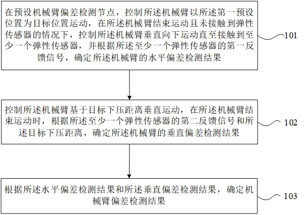
[0039] figure 1 A schematic flowchart of a method for detecting deviation of a robot arm of a semiconductor device provided by the present application. The semiconductor device includes a robot arm and two elastic sensors. The two elastic sensors are respectively disposed at the first detection point and the second detection point. The first detection point and the second detection point ar...


PUM


Abstract

The invention provides a deviation detection method and device for a mechanical arm of semiconductor equipment, and the semiconductor equipment comprises the mechanical arm and two elastic sensors which are respectively arranged at the left upper extreme position and the right lower extreme position or the left lower extreme position and the right upper extreme position of the bottom surface of the mechanical arm when the mechanical arm is located at a first preset position. The method comprises the steps that at a preset time point in the working process of the mechanical arm, the mechanical arm is controlled to move with a first preset position as a target position, and under the condition that the mechanical arm stops moving and does not make contact with elastic sensors, the mechanical arm is controlled to move downwards till making contact with at least one elastic sensor; a horizontal deviation detection result is determined according to a first feedback signal of the elastic sensor, the mechanical arm is controlled to vertically move based on the target pressing distance, a vertical deviation detection result is determined according to a second feedback signal of the elastic sensor, and a mechanical arm deviation detection result is determined according to the horizontal and vertical deviation detection results; and the deviation of the mechanical arm in the working process can be efficiently and timely detected.

Description

technical field [0001] The present application relates to the field of semiconductor technology, and in particular, to a method and device for detecting deviation of a robot arm of a semiconductor equipment. Background technique [0002] Semiconductor process equipment usually uses robotic arms to transfer wafers between various equipment components. In order to make full use of the internal space of the equipment, the various components inside the equipment will be arranged in the tightest way, and only limited movable parts such as robotic arms are reserved. activity space. Based on this, semiconductor processing equipment has very high requirements on the movement accuracy of the robot arm. If the movement accuracy of the robot arm is deviated, it will lead to accidents such as wafer transfer failure and the robot arm hitting other equipment components. However, the ultra-high temperature, vacuum or ultra-high pressure working environment in the semiconductor process equ...

Claims


Application Information

Patent Timeline
Patent Type & Authority Applications(China)
IPC IPC(8): B25J19/00
CPCB25J19/0095
Inventor 阮正华孙文彬
Owner 江苏邑文微电子科技有限公司
Features
  • R&D
  • Intellectual Property
  • Life Sciences
  • Materials
  • Tech Scout
  • Unparalleled Data Quality
  • Higher Quality Content
  • 60% Fewer Hallucinations
Learn More