Digital photoetching method of circuit board and digital photoetching system of circuit board applying digital photoetching method

A lithography system and circuit board technology, which is applied to microlithography exposure equipment, photolithographic process exposure devices, conveyor objects, etc., can solve the problems of single structure, time cannot be overlapped, low lithography efficiency, etc., and saves time, improving lithography efficiency, cost saving effect

Pending Publication Date: 2022-07-29
广东科视光学技术股份有限公司
View PDF10 Cites 2 Cited by
  • Summary
  • Abstract
  • Description
  • Claims
  • Application Information

AI Technical Summary

Problems solved by technology

The structure of the existing photolithography device is single, and the time for PCB circuit board loading, photolithography and PCB circuit board blanking cannot be overlapped, and the efficiency of photolithography is low

Method used


Image

  • Digital photoetching method of circuit board and digital photoetching system of circuit board applying digital photoetching method
  • Digital photoetching method of circuit board and digital photoetching system of circuit board applying digital photoetching method
  • Digital photoetching method of circuit board and digital photoetching system of circuit board applying digital photoetching method

Examples


Embodiment Construction

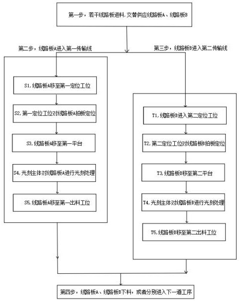
[0031] The technical solutions in the embodiments of the present invention will be clearly and completely described below with reference to the drawings in the embodiments of the present invention. Obviously, the described embodiments are only a part of the embodiments of the present invention, but not all of the embodiments. Based on the embodiments of the present invention, all other embodiments obtained by those of ordinary skill in the art without creative efforts shall fall within the protection scope of the present invention.

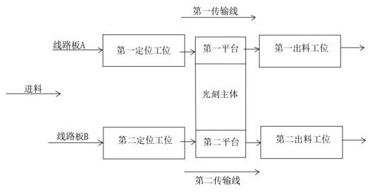
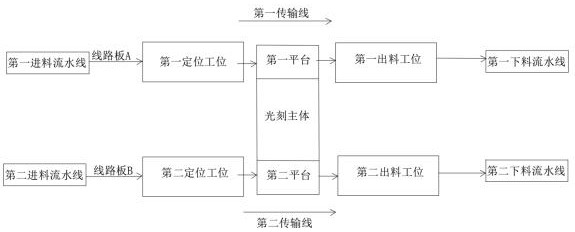
[0032] like figure 1 , figure 2 As shown, the present invention provides a digital lithography method for circuit boards, which is applied to a digital lithography system for circuit boards. The digital lithography system for circuit boards includes a lithography body, a first transmission line, and a second transmission line. The first transmission line includes a first positioning station, a first platform, and a first discharging station, the...


PUM


Abstract

The invention provides a digital photoetching method of a circuit board, a digital photoetching system of the circuit board comprises a photoetching main body, a first transmission line and a second transmission line, the first transmission line comprises a first positioning station, a first platform and a first discharging station, and the second transmission line comprises a second positioning station, a second platform and a second discharging station. The digital photoetching method of the circuit boards comprises the following steps: 1, feeding a plurality of circuit boards, and alternately supplying a circuit board A and a circuit board B; 2, the circuit board A enters a first transmission line; thirdly, the circuit board B enters the second transmission line, and the second step and the third step are carried out at the same time. According to the invention, the circuit board is shunted to the two transmission lines, and the photoetching main body alternately carries out digital photoetching treatment on the circuit boards on the two platforms, so that the photoetching efficiency is greatly improved, the time is saved, and the cost is saved.

Description

【Technical field】 [0001] The invention relates to the technical field of lithography of circuit boards, in particular to a digital lithography method of circuit boards and a digital lithography system of circuit boards using the same. 【Background technique】 [0002] Photolithography refers to the technology of transferring the pattern on the mask to the substrate with the help of photoresist (also known as photoresist) under the action of light. The main process is usually as follows: first, ultraviolet light is irradiated to the surface of the substrate with a layer of photoresist film through a mask, causing a chemical reaction of the photoresist in the exposed area, and then the exposed area or unexposed area is dissolved and removed by developing technology. The photoresist (the former is called positive photoresist, the latter is called negative photoresist), so that the pattern on the mask is copied to the photoresist film, and finally the pattern is transferred to the...

Claims


Application Information

Patent Timeline
Patent Type & Authority Applications(China)
IPC IPC(8): B65G47/68B65G47/71B65G47/91G03F7/20
CPCB65G47/681B65G47/71B65G47/912B65G47/918G03F7/70733
Inventor 王华陈志特
Owner 广东科视光学技术股份有限公司
Why Eureka
Try Eureka