
Optimal selection method of SRAM IP

An optimal selection and specification technology, applied in the direction of instrumentation, computing, electrical digital data processing, etc., can solve the problems of 128x80 small area, different area and power consumption, and different depth bit-width ratio, etc., to achieve optimal area, Optimum effect on power consumption

Pending Publication Date: 2022-07-29
芯河半导体科技(无锡)有限公司
View PDF0 Cites 0 Cited by
  • Summary
  • Abstract
  • Description
  • Claims
  • Application Information

AI Technical Summary

Problems solved by technology

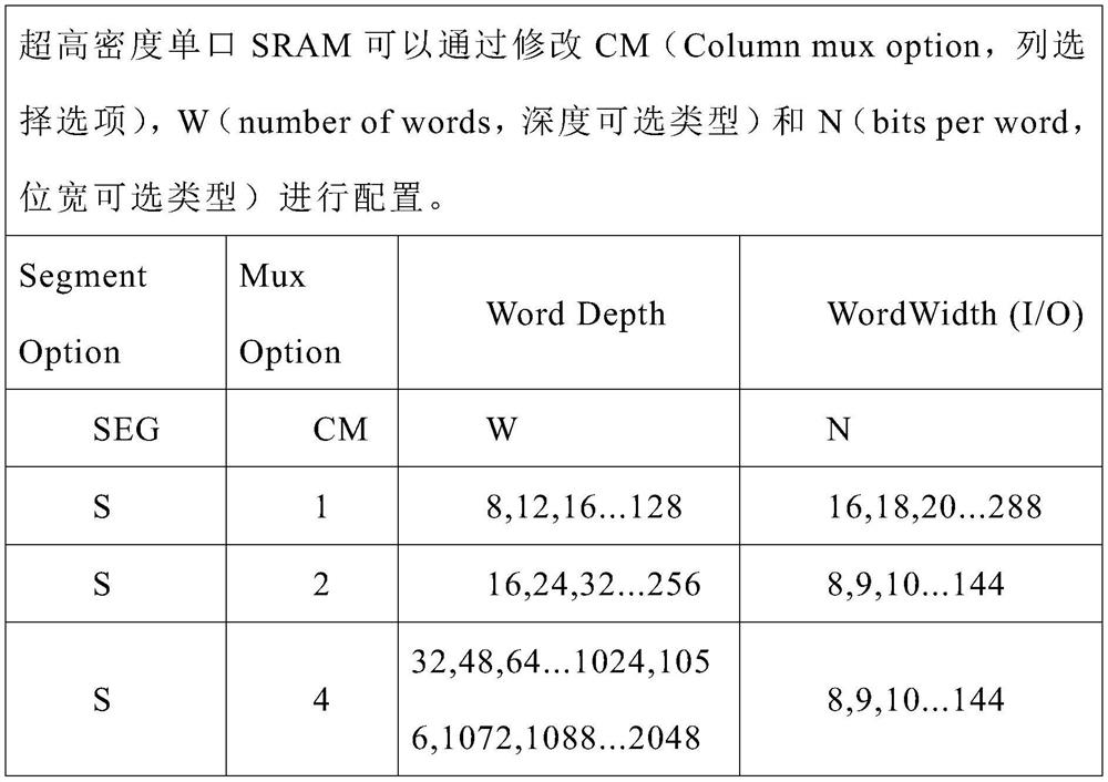
[0008] 2. For example, if you need an SRAM of 128x79 (depth 128bit, bit width 79bit), if you choose according to the specifications, you will choose 128x79 specifications, that is, CM=2 (CM is the CM column in the table) or 4 SRAM in the above figure, But in fact, it may be that the area of ​​128x80 in the CM=1 type is smaller
[0009] 3. Although SRAM is only a memory, the ratio of depth to bit width of SRAM with the same capacity is different, and its area and power consumption are also different.

Method used


Image

  • Optimal selection method of SRAM IP
  • Optimal selection method of SRAM IP
  • Optimal selection method of SRAM IP

Examples


Embodiment 1

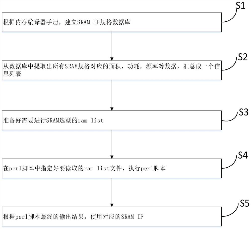
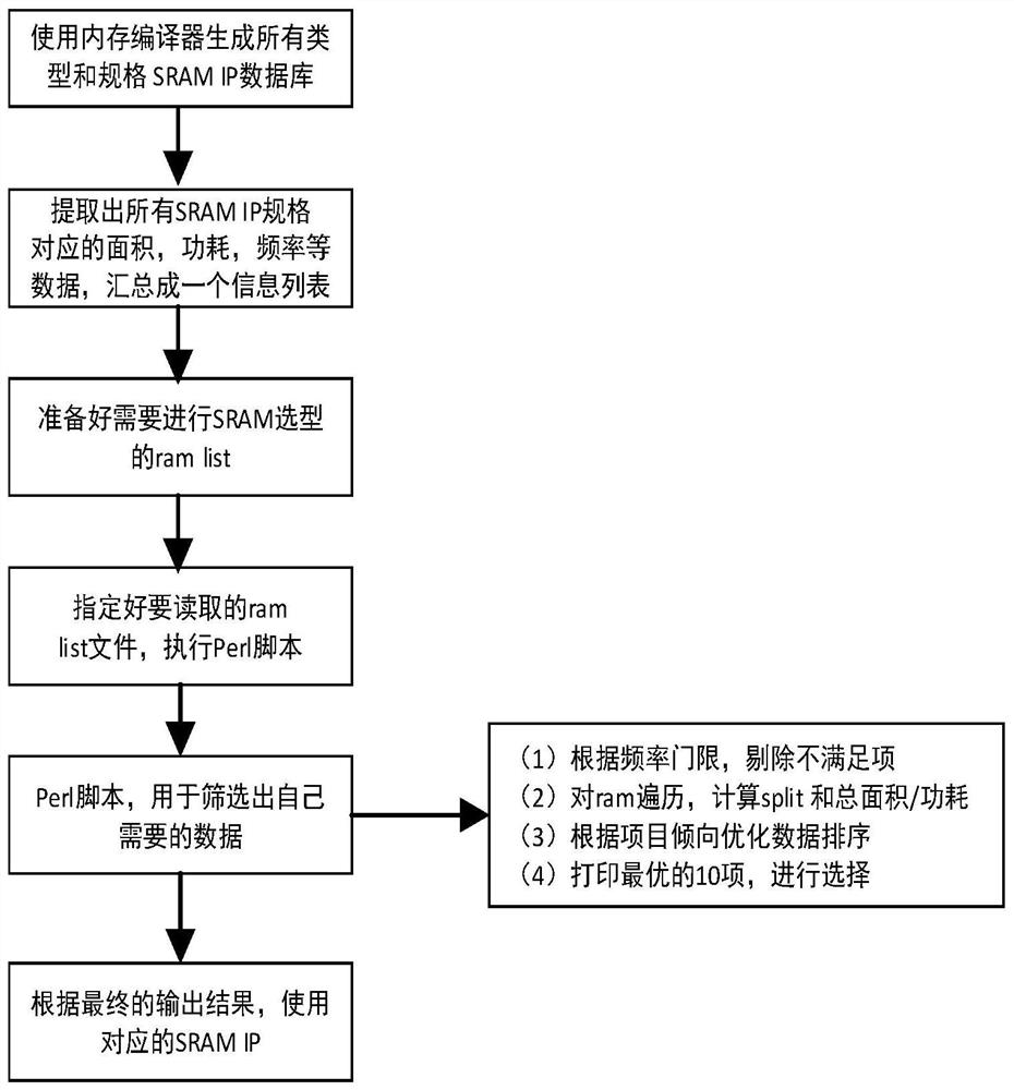
[0043] This embodiment is used to describe the specific implementation of an optimal selection method for SRAM IP, such as figure 2 The specific implementation steps are as follows:

[0044] S1 obtains all 1rw, 1r1w, 2rw specifications that can be generated by the required process according to the memory compiler manual provided by TSMC, and generates all SRAM IPs, and establishes a SRAM IP database;

[0045] The specifications include frequency, area, power consumption, depth optional range, bit width optional range, optional function (redundant bit), area and power consumption are the judgment conditions for selecting the optimal SRAM, and other specification conditions as demand.

[0046] S2 extracts the area, power consumption, frequency and other data corresponding to all SRAM specifications from the database, and summarizes them into an information list;

[0047] S3 prepares the ram list that needs to be selected for SRAM;

[0048] The ram list contains the SRAM IP n...


PUM


Abstract

According to the optimal selection method of the SRAM IP, an SRAM IP specification database is established according to data provided by a memory compiler, a screening rule and a sorting rule are set through a Perl script, and the SRAM with the optimal area or the optimal power consumption or the most balanced is automatically selected, so that the SRAM selection efficiency is improved, repeated labor is avoided, the chip verification efficiency is improved, and the chip verification efficiency is improved. And the labor cost is greatly saved.

Description

technical field [0001] The invention relates to the technical field of chip verification, in particular to an optimal selection method of SRAM IP. Background technique [0002] As the chip integration becomes higher and higher, area and power consumption become the bottleneck in many cases. As we all know, the chip manufacturing process is constantly improving, from 40nm to 28nm, 16nm, and 7nm, but each generation process has its own area limit. Exceeding this area limit will lead to a significant drop in chip yield, which will bring cost. Can not control. We all know the impact of large power consumption. For mobile phones, it means short standby time, and for home appliances, it consumes large amounts of power. [0003] At present, SRAM (SRAM: Static Random Access Memory) is used in most chips. As a chip designer, only the type, depth and bit width of SRAM will be proposed according to functional requirements. However, the area and function of SRAM are ultimately determi...

Claims


Application Information

Patent Timeline
IPC IPC(8): G06F30/398
CPCG06F30/398
Inventor 石鑫
Owner 芯河半导体科技(无锡)有限公司
Learn More