Modularized Pin-to-microstrip transition structure

A transitional structure and modularization technology, applied in waveguide-type devices, circuits, connecting devices, etc., can solve the problems of increasing the difficulty of circuit design and assembly, affecting the microstrip matching structure, and greatly affecting the processing error, so as to solve the problem of gold wire bonds. lower reliability, avoid discontinuities, and improve assembly tolerances

Pending Publication Date: 2022-08-02
石家庄烽瓷电子技术有限公司
View PDF0 Cites 2 Cited by
  • Summary
  • Abstract
  • Description
  • Claims
  • Application Information

AI Technical Summary

Problems solved by technology

Therefore, in practical applications, the microstrip at the end of the gold wire will be used for compensation, and often the compensation structure will be wider than the original microstrip line, which will affect the matching structure of the microstrip
And the gold wire bonding length between the Pin needle and the microstrip is limited by the extension height of the Pin needle and the horizontal distance from the Pin needle to the microstrip.
[0005] In general, the use of gold wire bonding for transition will not only affect the original matching structure, but also be greatly affected by processing errors, which increases the difficulty of circuit design and assembly

Method used


Image

  • Modularized Pin-to-microstrip transition structure
  • Modularized Pin-to-microstrip transition structure
  • Modularized Pin-to-microstrip transition structure

Examples


Embodiment Construction

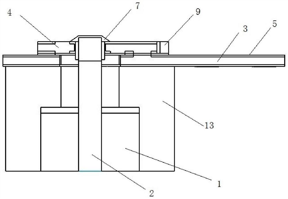
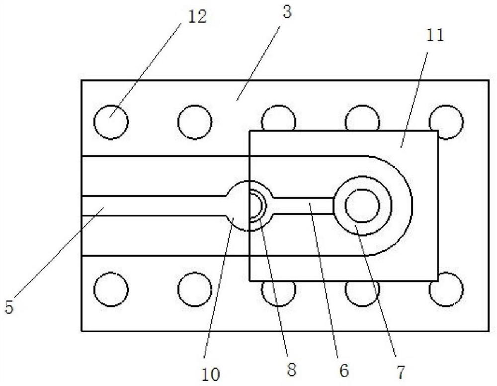
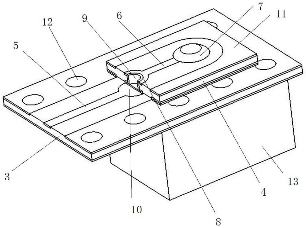
[0022] The technical solutions in the embodiments of the present invention will be clearly and completely described below with reference to the accompanying drawings in the embodiments of the present invention. Obviously, the described embodiments are only a part of the embodiments of the present invention, rather than all the embodiments. Based on the embodiments of the present invention, all other embodiments obtained by those of ordinary skill in the art without creative efforts shall fall within the protection scope of the present invention.

[0023] Many specific details are set forth in the following description to facilitate a full understanding of the present invention, but the present invention can also be implemented in other ways different from those described herein, and those skilled in the art can do so without departing from the connotation of the present invention. Similar promotion, therefore, the present invention is not limited by the specific embodiments dis...


PUM


Abstract

The invention discloses a modularized Pin-to-microstrip transition structure, which comprises a metal seat, a trapezoidal through hole is formed in the metal seat, a Pin is arranged in the through hole, an upper-layer substrate is fixed on the upper side of the metal seat, a transition substrate is arranged on the upper surface of the upper-layer substrate, and the metal seat is fixed on the transition substrate. An upper substrate through hole is formed in the position, corresponding to the through hole, of the upper substrate, a transition substrate through hole is formed in the portion, corresponding to the upper substrate through hole, of the transition substrate, the length of the transition substrate is smaller than that of the upper substrate, an upper substrate microstrip line is formed in the portion, on one side of the transition substrate, of the upper substrate, and a lower substrate microstrip line is formed in the portion, on the other side of the transition substrate, of the upper substrate. The upper end of the Pin is connected with one end of the microstrip line of the upper substrate through a metal structure located on the transition substrate. The transition structure has the advantages of high reliability, small size, low assembly difficulty and the like.

Description

technical field [0001] The invention relates to the technical field of electronic components, in particular to a modular pin-to-microstrip transition structure. Background technique [0002] With the increasing demand for miniaturized RF microsystems at home and abroad, RF systems are gradually changing from planar packaging to three-dimensional packaging, thereby improving the vertical integration of RF microsystems. With the emergence of the three-dimensional packaging structure, vertical interconnection devices between the upper and lower substrates are inevitably used. The devices usually used for the vertical interconnection between the boards include Pin pins and hair buttons. Pin pins are usually used for vertical connection of DC signals. Pin pins can be connected to the surface circuit of the upper board only through through holes on the upper board without designing other additional structures in the substrate. The vertical transmission of RF signals often adopts a...

Claims


Application Information

Patent Timeline
Patent Type & Authority Applications(China)
IPC IPC(8): H01P5/08
CPCH01P5/085
Inventor 陈子豪曾欣赖邱亮
Owner 石家庄烽瓷电子技术有限公司
Why Eureka
Try Eureka