Cold electron erase in thin film memory transistors
A storage transistor, electronic technology, applied in information storage, static memory, read-only memory, etc., can solve the problem of harmful persistence of storage transistors
- Summary
- Abstract
- Description
- Claims
- Application Information
AI Technical Summary
Problems solved by technology
Method used
Image

Examples
Embodiment Construction
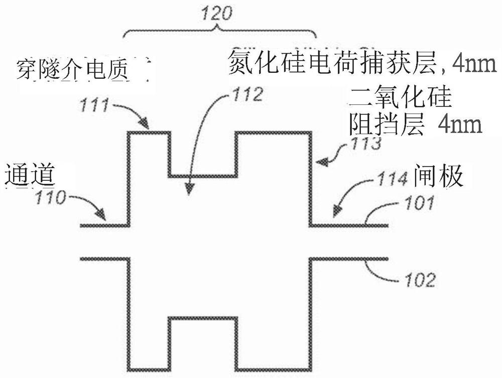
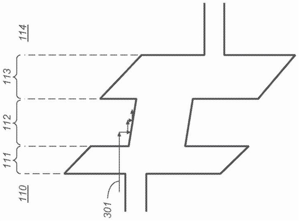
[0029] The present invention utilizes a device structure in a desired low energy range (referred to as "cold electrons") to ensure that electrons tunnel out of a charge trapping layer into the channel region of a memory transistor (eg, during an erase operation) so that the final The hole generation is also low energy, so there is less damage to the write window, improving the endurance of the memory transistor to more than 10 11 write-erase cycles. The device structure provides a substantial direct tunneling write current density in excess of 1.0 amps / cm 2 (eg 5.0amps / cm 2 ). The present invention is particularly advantageous for use with memory layers that form thin film memory transistors in three-dimensional memory structures, such as the quasi-volatile memory transistors previously described by Harari in three-dimensional arrays of inverse-OR gate memory strings.
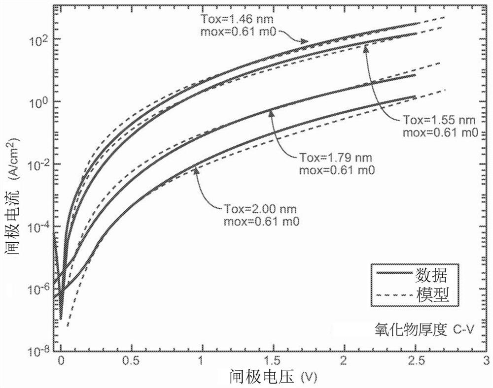
[0030] An embodiment of the present invention consists of Figure 5 , which shows conduction band bounda...
PUM
 Abstract
Description
Claims
Application Information
 - R&D Engineer
- R&D Manager
- IP Professional
- Industry Leading Data Capabilities
- Powerful AI technology
- Patent DNA Extraction
Browse by: Latest US Patents, China's latest patents, Technical Efficacy Thesaurus, Application Domain, Technology Topic.
© 2024 PatSnap. All rights reserved.Legal|Privacy policy|Modern Slavery Act Transparency Statement|Sitemap