Semiconductor device

A technology for semiconductors and devices, applied in the field of improved semiconductor devices, can solve problems such as short circuits between wiring layers and semiconductor substrates, and achieve the effect of preventing short circuits

Inactive Publication Date: 2004-05-12
MITSUBISHI ELECTRIC CORP
View PDF0 Cites 0 Cited by
  • Summary
  • Abstract
  • Description
  • Claims
  • Application Information

AI Technical Summary

Problems solved by technology

As a result, a so-called short-circuit problem occurs between a wiring layer and a wiring layer of a different potential, or between a wiring layer and a semiconductor substrate.

Method used


Image

  • Semiconductor device
  • Semiconductor device
  • Semiconductor device

Examples


Embodiment Construction

[0019] Next, embodiments of the present invention will be described with reference to the drawings.

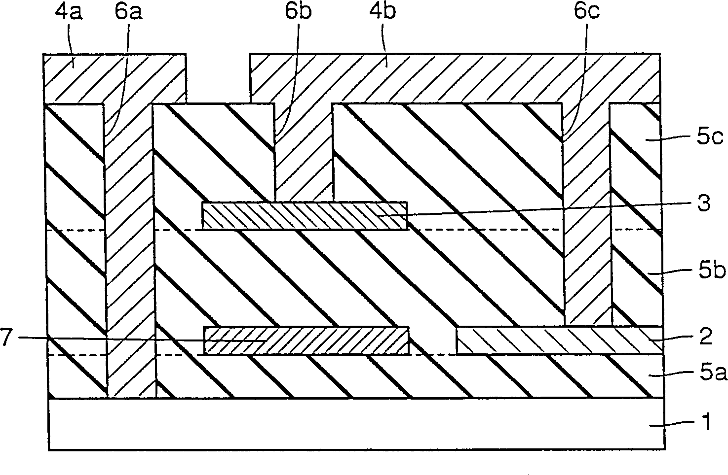
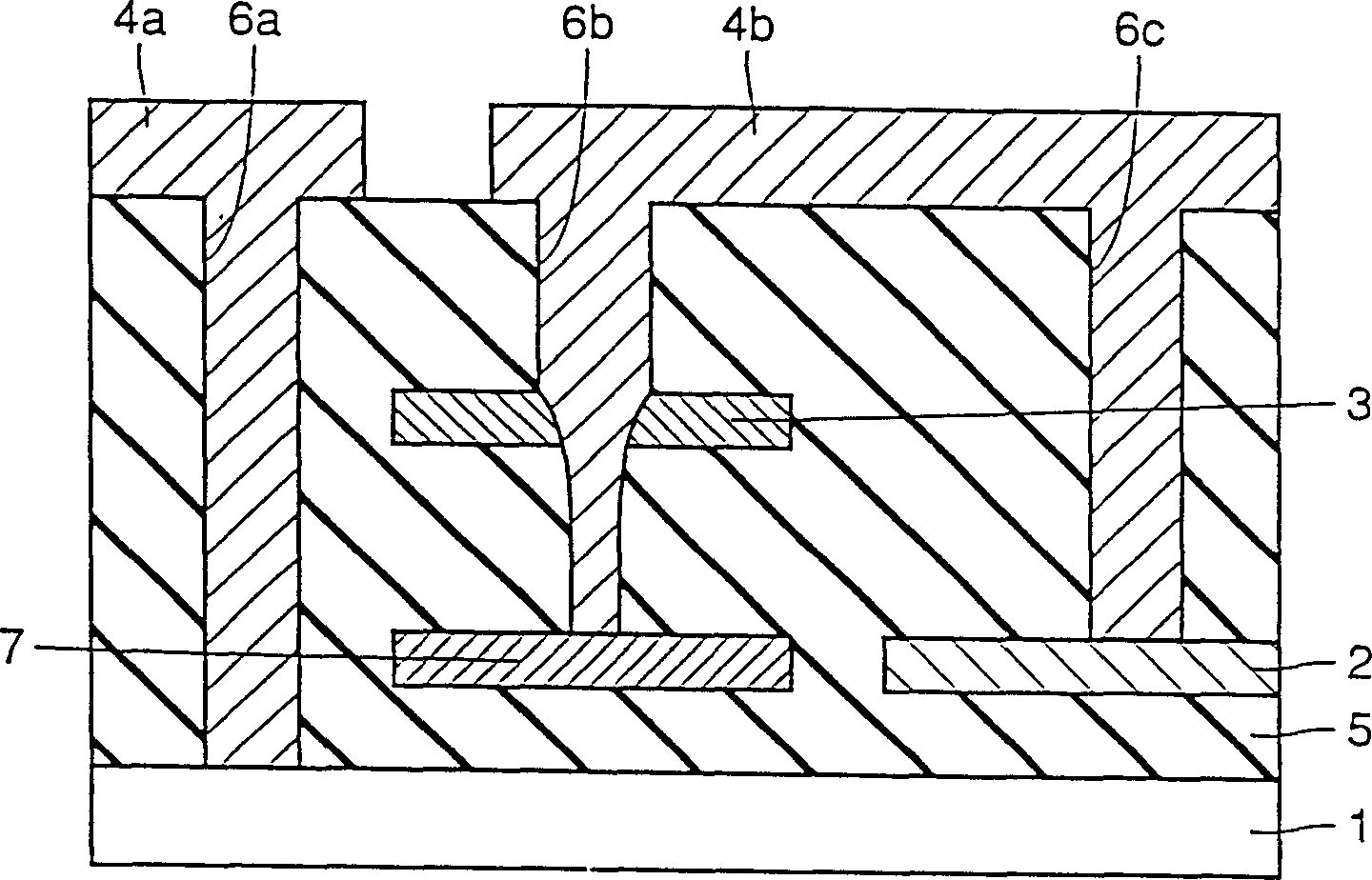
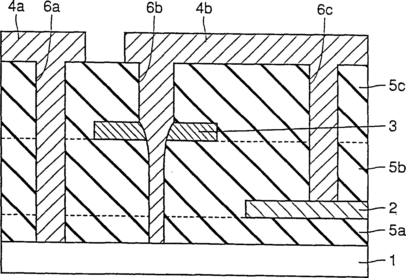
[0020] figure 1 is a cross-sectional view of a semiconductor device of an embodiment of the present invention. The semiconductor device is provided with a semiconductor substrate 1 . A first interlayer insulating film 5 a is provided on the semiconductor substrate 1 . The first conductive layer 2 and the barrier layer 7 are provided on the first interlayer insulating film 5a. Next, the barrier layer 7 will be described.

[0021] An interlayer insulating film 5 b is provided on the interlayer insulating film 5 a so as to cover the first conductive layer 2 and the barrier layer 7 . The second conductive layer 3 is provided on the interlayer insulating film 5b. An interlayer insulating film 5 c is provided on the interlayer insulating film 5 b so as to cover the second conductive layer 3 . In the interlayer insulating films 5a, 5b, and 5c, contact holes 6a for exposing the...


PUM


Abstract

An improved semiconductor device which prevents a short circuit between a wiring layer and a semiconductor substrate, caused by the penetration of a contact hole, will be provided. A lower conducting layer is formed on a second interlayer insulating film. A third interlayer insulating film covers lower conducting layer. A contact hole is formed in third interlayer insulating film in order to connect an upper conducting layer and lower conducting layer. A stopper layer of silicide or metal is formed below contact hole between the surface of a semiconductor substrate and lower conducting layer.

Description

technical field [0001] The present invention relates generally to semiconductor devices, and more particularly to an improved semiconductor device comprising a wiring layer capable of preventing the wiring layer from being short-circuited to a wiring layer of a different potential or to a semiconductor substrate. Background technique [0002] image 3 It is a sectional view of a conventional semiconductor device such as a semiconductor memory having a multilayer wiring structure. [0003] refer to image 3 , an interlayer insulating film 5 a is provided on the semiconductor substrate 1 . The first conductive layer 2 is provided on the interlayer insulating film 5a. An interlayer insulating film 5 b is provided on the interlayer insulating film 5 a so as to cover the first conductive layer 2 . The second conductive layer 3 is provided on the interlayer insulating film 5b. An interlayer insulating film 5 c is provided on the interlayer insulating film 5 b so as to cover the...

Claims


Application Information

Patent Timeline
IPC IPC(8): H01L21/768H01L23/522
CPCH01L23/5226H01L2924/0002H01L2924/00H01L21/28
Inventor 豆谷智治永井享浩
Owner MITSUBISHI ELECTRIC CORP
Why Eureka
Try Eureka