
Eureka
For R&D, Eureka makes reading and utilizing patents & technical documents easy.
Eureka AIR
Designed for self-driven R&D workflows. Generate viable solutions, solve complex R&D challenges, empower your innovation with AI.

Eureka Materials
Designed for material experts only. Revolutionize your material R&D, from search, analyze, to developing new materials.

TechResearch
Generate reliable direction feasibility study reports for your R&D in just a few steps.

TechSeek
Discover and master advanced knowledge NOW. Basics, ideas, possibilities, all at once.

TechMind
As an expert in R&D Theories, TechMind can generates customized viable solutions instantly.

TechRisk
Analyze your overall solution with one click, know your potential R&D risks in advance.

TechMonitor
Get weekly tech updates, stay abreast of the latest tech innovations and key insights.
Organic electroluminescent display device
A technology of electroluminescent display and electroluminescent materials, which is applied in the direction of electroluminescent light sources, electric light sources, circuits, etc., and can solve problems such as differences in brightness and current density
- Summary
- Abstract
- Description
- Claims
- Application Information
AI Technical Summary
Problems solved by technology
Method used
Image

Examples
Embodiment Construction
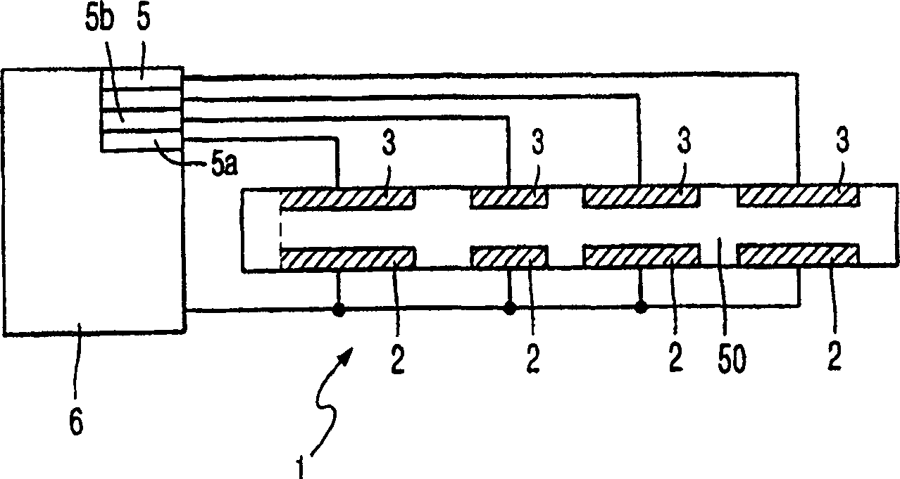
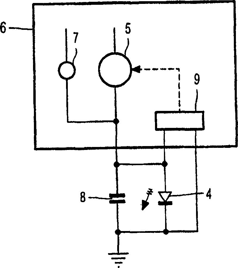
[0026] figure 1 A display device 1 is shown with an active layer 50 between the two modes of electrode layers 2, 3 of conductive material. In this example, the electrode 2 and the electrode 3 and the active material in the middle position are defined as a light emitting diode (LED) 4, which is also called a pixel. At least one of the electrode patterns is transparent to the light emitted in the active layer. During operation, the electrode 2 is driven in such a way. With respect to the electrode 3, they have a sufficient positive voltage for injecting holes into the active layer. The materials of these electrodes 2 have high working functions, and are usually composed of indium oxide or indium-tin oxide (ITO) layers. ITO is particularly suitable due to its satisfactory conductivity and high transparency. Electrode 3 serves as a negative electrode (as opposed to electrode 2) for injecting electrons into the active layer. In this example, the material used for this layer is alumin...
PUM
 Abstract
Description
Claims
Application Information
 - R&D Engineer
- R&D Manager
- IP Professional
- Industry Leading Data Capabilities
- Powerful AI technology
- Patent DNA Extraction
Browse by: Latest US Patents, China's latest patents, Technical Efficacy Thesaurus, Application Domain, Technology Topic, Popular Technical Reports.
© 2024 PatSnap. All rights reserved.Legal|Privacy policy|Modern Slavery Act Transparency Statement|Sitemap|About US| Contact US: help@patsnap.com