Electrostatic discharge protective circuit having high trigger current

An electrostatic discharge protection and trigger current technology, applied in circuits, electrical components, electrical solid devices, etc., can solve the problems of unacceptable or sending signals, small trigger current, latching, etc., to avoid latching effect, good ESD The effect of protective ability

Inactive Publication Date: 2006-03-29
WINBOND ELECTRONICS CORP
View PDF0 Cites 0 Cited by
  • Summary
  • Abstract
  • Description
  • Claims
  • Application Information

AI Technical Summary

Problems solved by technology

[0003] However, by figure 2 The trigger current I of the traditional SCR can also be known from the volt-ampere characteristic diagram in trig is also very small
In this way, when a bonding pad uses a traditional SCR as an ESD protection component, under normal power supply conditions, it is easily triggered by noise interference, and a latch-up phenomenon occurs, so that the bonding pad 13 will be clamped at a fairly low potential (~V hold ), and cannot accept or send signals

Method used


Image

  • Electrostatic discharge protective circuit having high trigger current
  • Electrostatic discharge protective circuit having high trigger current
  • Electrostatic discharge protective circuit having high trigger current

Examples


Embodiment Construction

[0024] In order to make the above-mentioned purposes, features and advantages of the present invention more obvious and understandable, a preferred embodiment is specifically cited below, together with the attached Figure 3-9 , as detailed below:

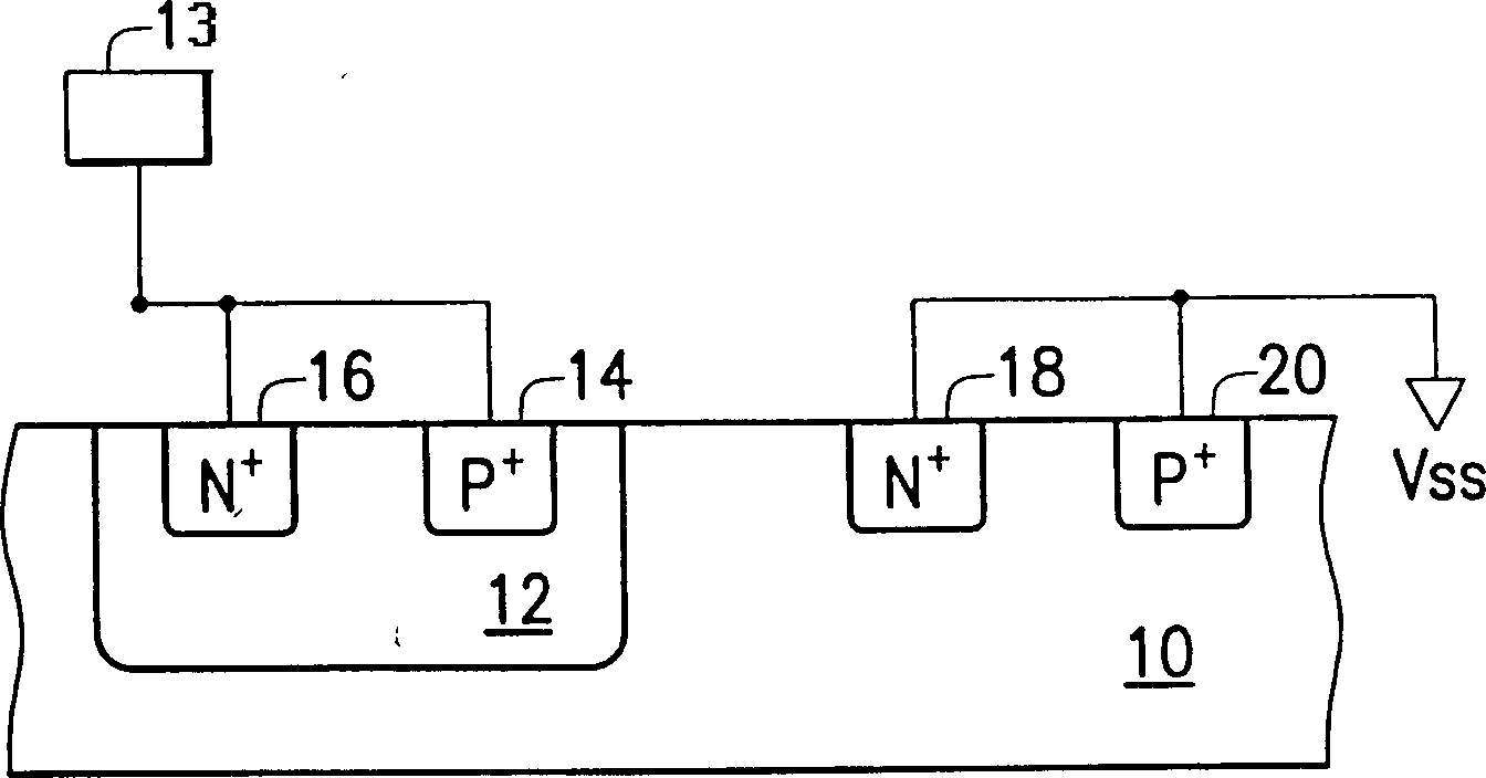
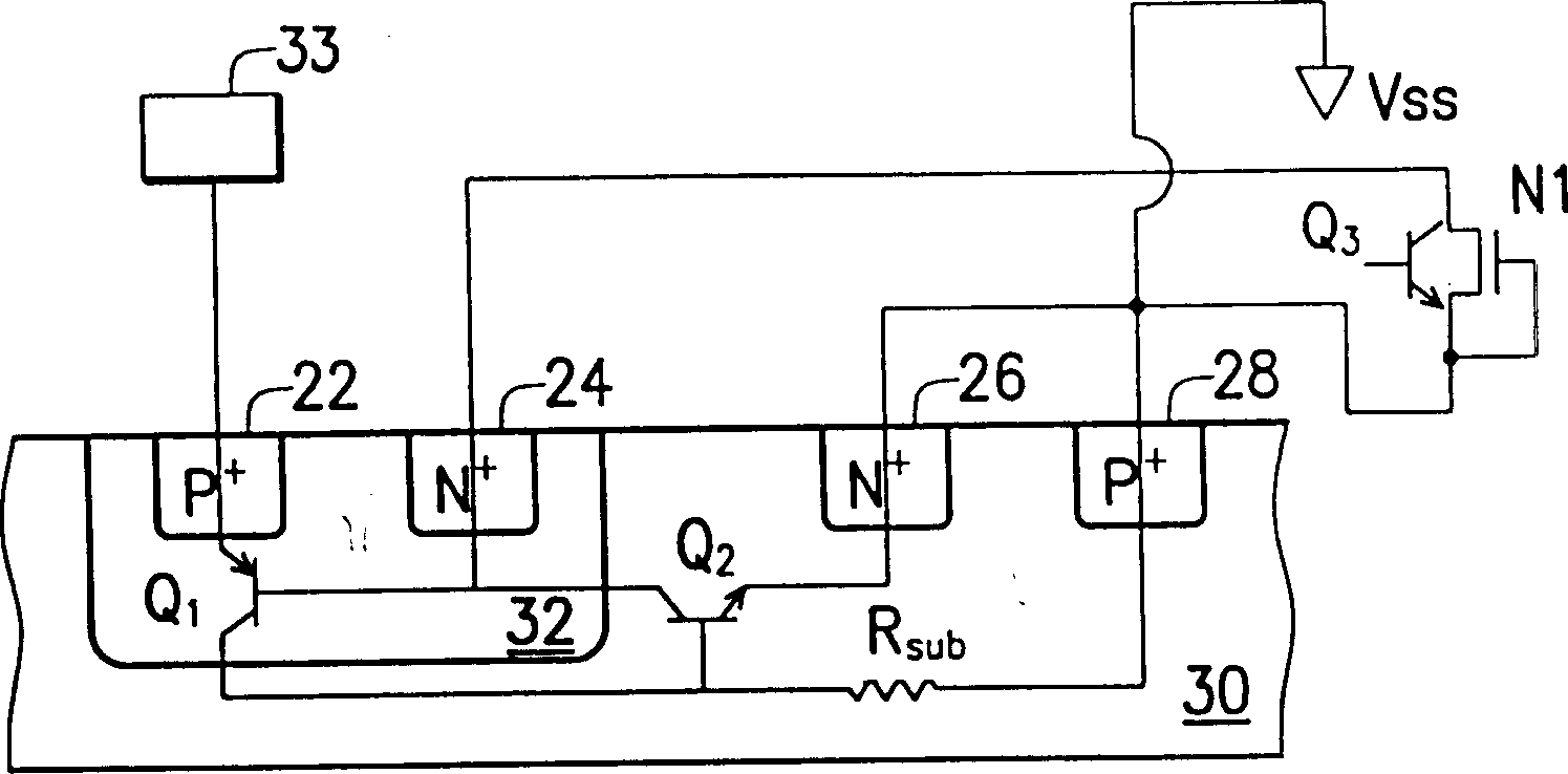
[0025] image 3 It is a schematic cross-sectional view of the ESD protection circuit of the present invention. Figure 4 for image 3 A layout diagram of the SCR shown.

[0026] image 3 Among them, the ESD protection circuit of the present invention mainly includes two components, one is a lateral SCR, and the other is an NMOS N1. Such as image 3 , Figure 4 As shown, the P+ doped region 22, the N-type well 32, the P-type substrate 30 and the N+ doped region 26 constitute the PNPN structure of the lateral SCR, which are respectively used as the anode, the positive gate, the negative gate and the lateral SCR of the lateral SCR. cathode. The P+ doped region 22 is directly coupled to a bonding pad 33 . The P-type substrate ...


PUM


Abstract

The electrostatic protecting circuit includes one semiconductor controlled rectifier (SCR) and one bipolar transistor in MOS structure. The SCR includes one anode, one anode/grid, one cathode/grid and one cathode, the anode is coupled to the first joint soldering pad, and the cathode/grid and the cathode are coupled to the second soldering pad. The bipolar transistor has one collector and one emitter, of which one is coupled to the anode/grid and the other to the second joint soldering pad. The electrostatic protecting circuit has relatively great triggering current to block the SCR, so that it can avoid accident blocking caused by noise during normal operation.

Description

technical field [0001] The present invention relates to an electrostatic discharge (ESD) protection circuit using a semiconductor controlled rectifier (SCR), especially an ESD protection circuit with high trigger current. Background technique [0002] ESD has been one of the important reliability measurement standards in semiconductor products, especially for downsized complementary metal oxide semiconductor (complementary metal oxide semiconductor, CMOS) technology. Because the breakdown voltage of the gate oxide layer of metal oxide semiconductor transistors (metal oxide semiconductor, MOS) becomes lower with the progress of manufacturing technology, therefore, setting up an ESD protection circuit at each input and output port is to prevent ESD stress from affecting gate oxidation. One of the effective ways to cause damage to layers. Because of its very low holding voltage, SCRs are often used as ESD protection components. figure 1 It is a schematic cross-sectional view ...

Claims


Application Information

Patent Timeline
Patent Type & Authority Patents(China)
IPC IPC(8): H01L23/60H01L27/00
Inventor 陈伟梵
Owner WINBOND ELECTRONICS CORP
Why Eureka
Try Eureka