Supercharge Your Innovation With Domain-Expert AI Agents!

Semiconductor device and display device

A technology of semiconductors and thin film transistors, applied in the field of circuit construction of driven components, can solve problems such as low luminous brightness

Inactive Publication Date: 2006-07-12
SANYO ELECTRIC CO LTD
View PDF0 Cites 0 Cited by
  • Summary
  • Abstract
  • Description
  • Claims
  • Application Information

AI Technical Summary

Problems solved by technology

In addition, in a region where the distance from the driving power supply Pvdd is long and the voltage drop due to the wiring resistance of the driving power supply line VL is significant, for example, in a pixel located far from the power supply, the voltage of the driving power supply line VL is low. And the luminance of each organic EL element 50 is lower than that of the elements close to the power source.

Method used


Image

  • Semiconductor device and display device
  • Semiconductor device and display device
  • Semiconductor device and display device

Examples


Embodiment Construction

[0063] Hereinafter, the best mode for carrying out the present invention (hereinafter referred to as embodiment) will be described with reference to the drawings.

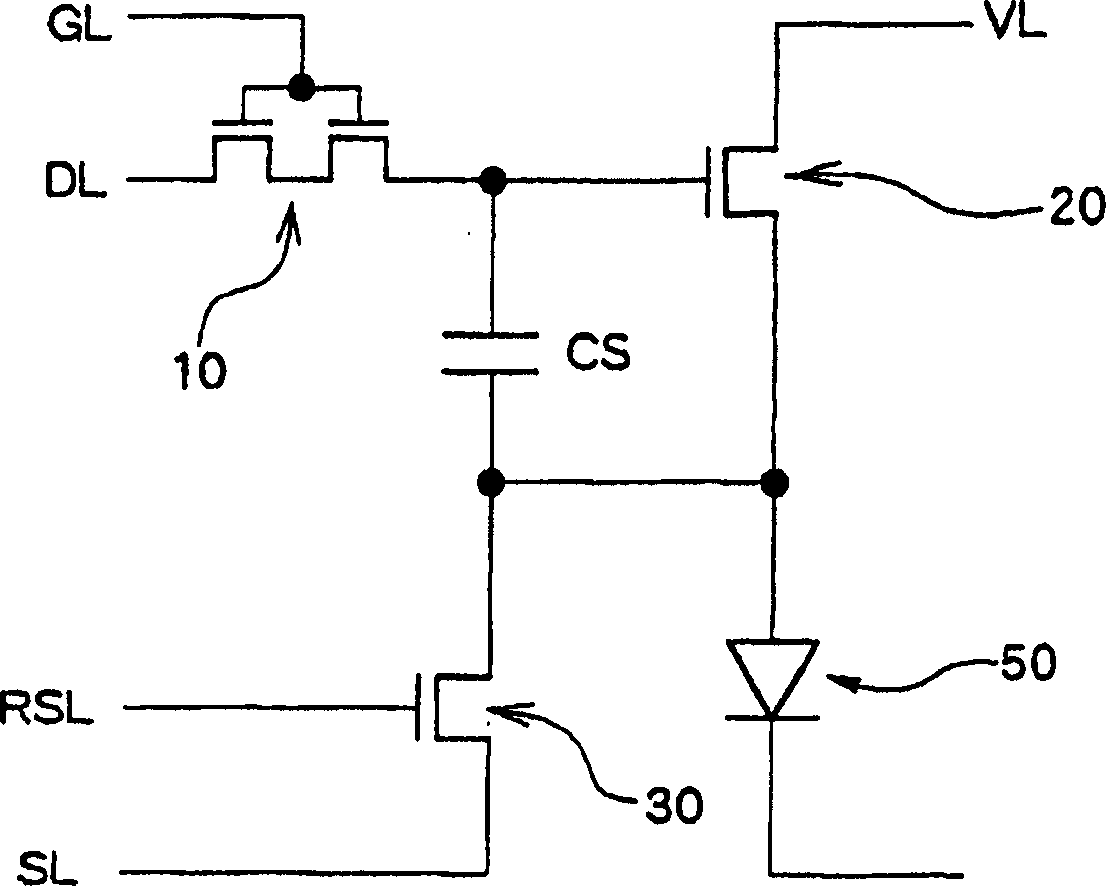
[0064] figure 1 A circuit configuration for driving an organic EL element according to an embodiment of the present invention is shown. In addition, here, the circuit configuration of one pixel in an active matrix organic EL display device will be specifically described by way of example.

[0065] 1 pixel as figure 1 As shown, it is equipped with an organic EL element 50 as a driven element or a display element, a switching thin film transistor (first TFT) 10, an element driving thin film transistor (second TFT) 20, and a storage capacitor Cs, and also has a reset thin film The transistor (third TFT) 30 serves as a switching element for resetting.

[0066] The first TFT 10 here is composed of nch-TFTs, its gate electrode is connected to the gate line GL, its drain is connected to the data line DL, and its sour...


PUM


Abstract

A semiconductor device for individually controlling an element to be driven, such as an electroluminescence element, includes a switching TFT which operates when a selection signal is applied to its gate and which also captures a data signal, and an element-driving TFT in which its drain is connected with a drive power source, its source is connected with the element to be driven, gate receives a data signal supplied from the switching TFT, for controlling electric power supplied from the drive power source to the element to be driven. The semiconductor device further includes a storage capacitor having a first electrode connected with the switching TFT and with the gate of the element-driving TFT and a second electrode connected between the source of the element-driving TFT and the element to be driven, for holding the gate-source voltage of the element-driving TFT in accordance with the data signal, and a switching element for controlling the potential of the second electrode of the storage capacitor. With such a configuration, all the above-described switches can be formed by TFTs of the same conductivity type and reliable supply of electric power to the element to be driven can be assured.

Description

technical field [0001] The present invention relates to a circuit configuration for controlling driven elements such as electroluminescent display elements. Background technique [0002] An EL display device that uses a self-luminescence element (Electroluminescence: EL) element for each pixel as a light-emitting element is not only self-luminous, but also has the advantages of thinness and low power consumption. It is used as an alternative to liquid crystal Display devices such as display devices (LCDs) and CRTs have attracted attention, and research on them is still ongoing. [0003] In addition, an active matrix EL display device in which a switching element such as a thin film transistor (TFT) for individually controlling the EL element is provided in each pixel, and the EL element is controlled for each pixel is expected as a high-precision display device. . [0004] Figure 13 Circuit configuration of each pixel in an active matrix EL display device displaying m row...

Claims


Application Information

Patent Timeline
Patent Type & Authority Patents(China)
IPC IPC(8): G09G3/32H01L27/32
CPCH01L27/3244G09G2300/0861G09G2300/0852G09G2300/0809G09G3/3266G09G2310/0251G09G2320/0233G09G2320/043G09G3/3233G09G2300/0426G09G2300/0842G09G2300/0465H10K59/12G09G3/30
Inventor 松本昭一郎佐野景一
Owner SANYO ELECTRIC CO LTD
Features
  • R&D
  • Intellectual Property
  • Life Sciences
  • Materials
  • Tech Scout
  • Unparalleled Data Quality
  • Higher Quality Content
  • 60% Fewer Hallucinations
Learn More