Semiconductor memory
A memory and semiconductor technology, applied in static memory, read-only memory, digital memory information, etc., can solve the problem of increasing off-state leakage current of transistors, and achieve the effect of realizing storage capacity and realizing large-scale
- Summary
- Abstract
- Description
- Claims
- Application Information
AI Technical Summary
Problems solved by technology
Method used
Image

Examples
Embodiment 1
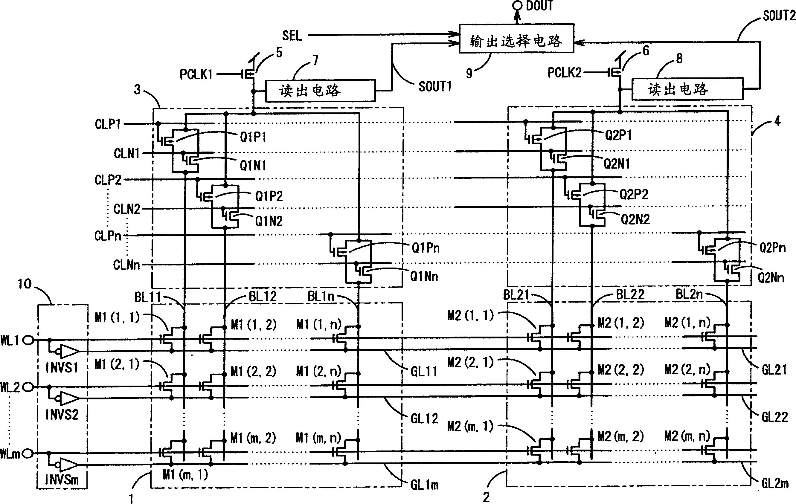
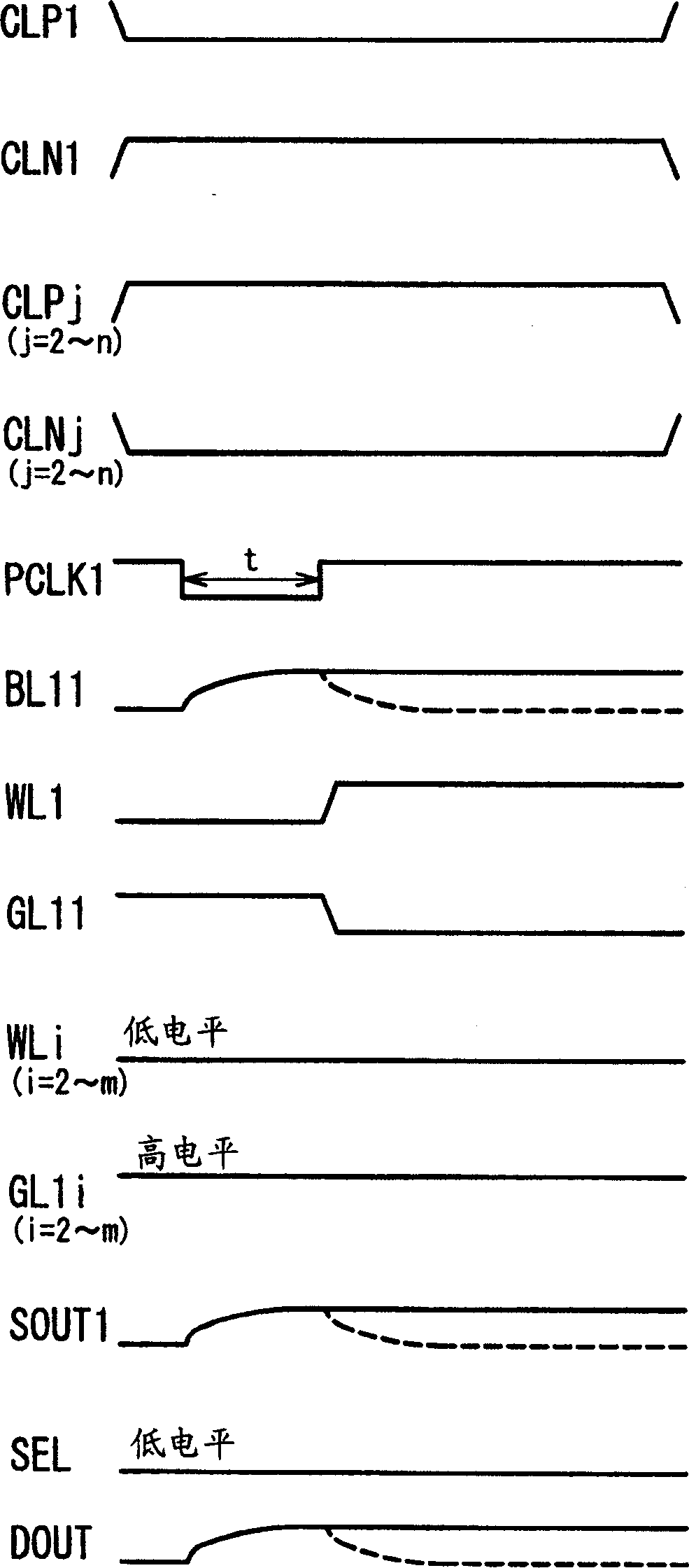
[0091] figure 1 It is a circuit diagram of the structure of the semiconductor memory device of the first embodiment of the present invention.
[0092] exist figure 1 Among them, the semiconductor memory is composed of memory cell arrays 1, 2, column decoders 3, 4, precharge transistors 5, 6, readout circuits 7, 8, output selection circuit 9, and source potential control circuit 10. The memory cell arrays 1 and 2, the column decoders 3 and 4, the precharge transistors 5 and 6, the readout circuits 7 and 8, and the output selection circuit 9 are the same as those of the conventional example, so the same reference numerals are assigned to the same members and omitted. illustrate.
[0093] The source potential control circuit 10 is composed of an NOT gate INVSi (i=1 to m). The input ends of the "not" gate INVSi (i=1~m) are respectively connected to the word line terminals WLi (i=1~m), and the output ends are respectively connected to the source lines GL1i (i=1~m) and On the ...
no. 2 Embodiment
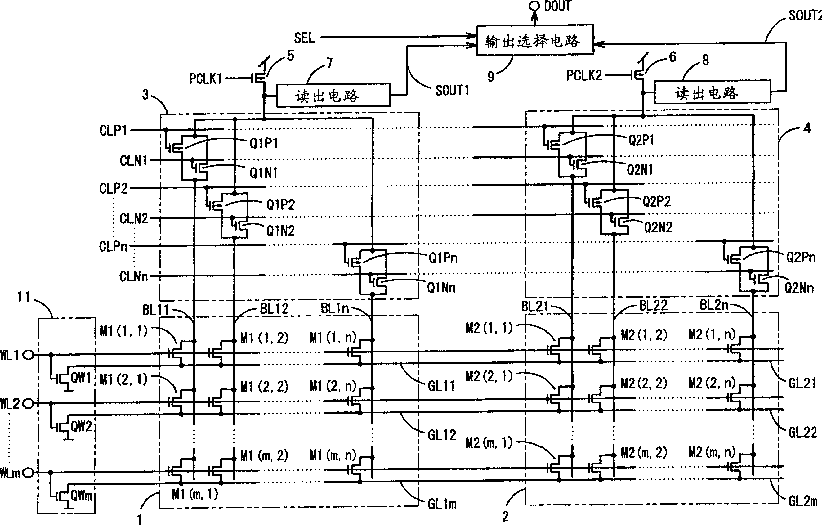
[0101] image 3 It is a circuit diagram of the structure of the semiconductor memory device of the second embodiment of the present invention.
[0102] exist image 3 Among them, the semiconductor memory is composed of memory cell arrays 1, 2, column decoders 3, 4, precharge transistors 5, 6, readout circuits 7, 8, output selection circuit 9, and source potential control circuit 11. The memory cell arrays 1 and 2, the column decoders 3 and 4, the precharge transistors 5 and 6, the readout circuits 7 and 8, and the output selection circuit 9 are the same as those of the conventional example, so the same reference numerals are assigned to the same members and omitted. illustrate.
[0103] The source potential control circuit 11 is composed of N-type MOS transistors QWi (i=1 to m). The gates of N-type MOS transistors QWi (i=1~m) are respectively connected to word line terminals WLi (i=1~m), and the drains are respectively connected to source lines GL1i (i=1~m) and On the sour...
no. 3 Embodiment
[0112] Figure 5 It is a circuit diagram of the structure of the semiconductor memory device of the third embodiment of the present invention.
[0113] exist Figure 5 Among them, the semiconductor memory is composed of memory cell arrays 1, 2, column decoders 3, 4, precharge transistors 5, 6, readout circuits 7, 8, output selection circuit 9, and source potential control circuit 12. The memory cell arrays 1 and 2, the column decoders 3 and 4, the precharge transistors 5 and 6, the readout circuits 7 and 8, and the output selection circuit 9 are the same as those of the conventional example, so the same reference numerals are assigned to the same members and omitted. illustrate.
[0114] The source potential control circuit 12 is composed of an NOT gate INVGi (i=1-m), an N-type MOS transistor QWVi (i=1-m), and an N-type MOS transistor QWGi (i=1-m). The input ends of the "invert" gate INVGi (i=1~m) are respectively connected to the word line terminals WLi (i=1~m), and the ou...
PUM
 Abstract
Description
Claims
Application Information
 - R&D
- Intellectual Property
- Life Sciences
- Materials
- Tech Scout
- Unparalleled Data Quality
- Higher Quality Content
- 60% Fewer Hallucinations
Browse by: Latest US Patents, China's latest patents, Technical Efficacy Thesaurus, Application Domain, Technology Topic, Popular Technical Reports.
© 2025 PatSnap. All rights reserved.Legal|Privacy policy|Modern Slavery Act Transparency Statement|Sitemap|About US| Contact US: help@patsnap.com