Check patentability & draft patents in minutes with Patsnap Eureka AI!

Matrix array devices with flexible substrates

A flexible substrate and device technology, applied in the field of matrix array devices, can solve problems such as damage

Inactive Publication Date: 2006-10-11
KONINKLIJKE PHILIPS ELECTRONICS NV
View PDF2 Cites 0 Cited by
  • Summary
  • Abstract
  • Description
  • Claims
  • Application Information

AI Technical Summary

Problems solved by technology

[0005] However, when bending or flexing the device, especially when not bending around a single axis, such as when making the device part-spherical, damage is often caused

Method used


Image

  • Matrix array devices with flexible substrates
  • Matrix array devices with flexible substrates
  • Matrix array devices with flexible substrates

Examples


Embodiment Construction

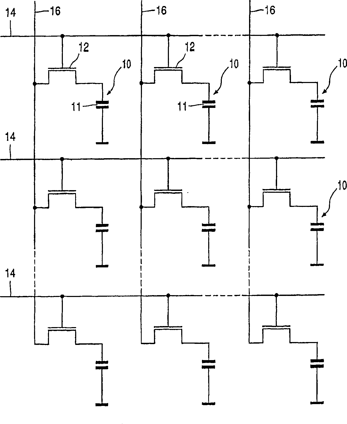
[0022] refer to figure 1 An active matrix liquid crystal display device (AMLCD) comprises a regular array of rows and columns of display pixels 10 , each display pixel 10 comprising a liquid crystal display element 11 and an associated thin film transistor TFT 12 . Individual pixels are arranged adjacent to the intersection of each set of row and column address conductors 14 and 16. In use, select (gate) and data signals are fed to address conductors 14 and 16, respectively, by peripheral driver circuitry (not shown). 16, in order to drive the pixels and make their display elements produce the desired display output.

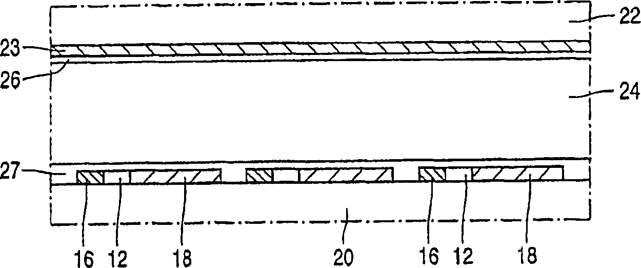
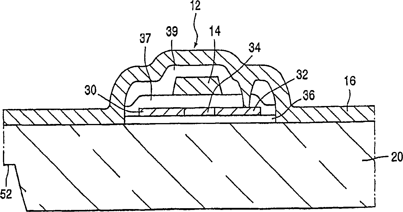
[0023] refer to figure 2 , each group of address conductors 14 and 16, TFT 12, and each pixel (display element) electrode 18 together constitute a thin film active matrix circuit, which is carried on the flat surface of a substrate 20 of flexible and pliable polymer material , and is made by depositing and patterning appropriate layers of conductive, insulati...


PUM


Abstract

A matrix array device, for example, an active matrix display device, image sensor, or the like, comprises a matrix circuit ( 12, 14, 16, 18 ) carried on a flexible substrate ( 20 ) which circuit includes an array of semiconductor devices ( 12 ), such as TFTs, occupying discrete areas. Selected regions of the substrate ( 20 ) away from the semiconductor devices ( 12 ) are formed as areas of weakness to encourage flexing of the substrate to occur preferentially at those regions upon bending of the device and so reduce the risk of damage to the semiconductor devices. The regions, for example, may comprise lines of weakness ( 50, 52 ) extending between the semiconductor devices and may be formed by localized thinning of the substrate or by treating the substrate material to modify its stiffness at predetermined areas.

Description

technical field [0001] The present invention relates to a matrix array device comprising a thin film matrix circuit comprising semiconductor devices carried on a flexible substrate. The device may be an image sensor, or a flat panel display such as a liquid crystal display, or other types of large area matrix electronics such as thin film data storage devices, thermal imaging devices, or touch or fingerprint readout sensing array devices. Background technique [0002] Currently, there is great interest in developing thin film matrix circuits with thin film transistors (TFTs), thin film photodiodes, or other semiconductor circuit elements on inexpensive substrates for large area electronic applications. In the development of flexible devices using flexible substrates such as insulating polymer materials or metal foils instead of conventional glass, to provide for example curved displays or other matrix array devices, for ergonomic design, aesthetic, or other reasons instead o...

Claims


Application Information

Patent Timeline
IPC IPC(8): H01L29/786H01L21/84H01L27/12G02F1/1333G02F1/1368G06K9/00G09F9/30H01L27/146
CPCG02F1/133305H01L29/78603G06V40/1306G02F1/133
Inventor N·D·杨
Owner KONINKLIJKE PHILIPS ELECTRONICS NV
Features
  • R&D
  • Intellectual Property
  • Life Sciences
  • Materials
  • Tech Scout
  • Unparalleled Data Quality
  • Higher Quality Content
  • 60% Fewer Hallucinations
Learn More