Process for pattern transfer

A technology of pattern transfer and pattern light, which is applied in the direction of photographic process, optics, and optomechanical equipment on the pattern surface, can solve the problem of not being able to effectively solve the problem of missing, not applicable to semiconductor and related semiconductor manufacturing processes, and increasing the critical dimension of pattern formation And other issues

Inactive Publication Date: 2006-11-22
FUJIAN JINHUA INTEGRATED CIRCUIT CO LTD
View PDF11 Cites 0 Cited by
  • Summary
  • Abstract
  • Description
  • Claims
  • Application Information

AI Technical Summary

Problems solved by technology

Obviously, although increasing the thickness of the patterned photoresist 13 is an easy and low-cost method, it will also increase the critical dimension of the pattern, so it is not suitable for semiconductors that require fine patterns and related semiconductor processes.
[0006] To sum up, the conventional technology cannot effectively solve the loss caused by the etching of the photoresist material in the pattern transfer process, especially it cannot provide a low-cost solution suitable for fine patterns

Method used


Image

  • Process for pattern transfer
  • Process for pattern transfer
  • Process for pattern transfer

Examples


Embodiment Construction

[0016] In view of the various defects encountered in the conventional technology when changing the photoresist material and increasing the thickness of the photoresist to increase the etching resistance of the photoresist, the present invention proposes the following entry points:

[0017] (1) As long as the etching resistance of a certain material is large enough, the damage caused by etching can be effectively prevented without increasing the thickness of the material.

[0018] (2) As long as there is a material with a large enough etching resistance on the surface of the photoresist, which can offset the effect of the etching process on the photoresist, the material of the photoresist can not be changed.

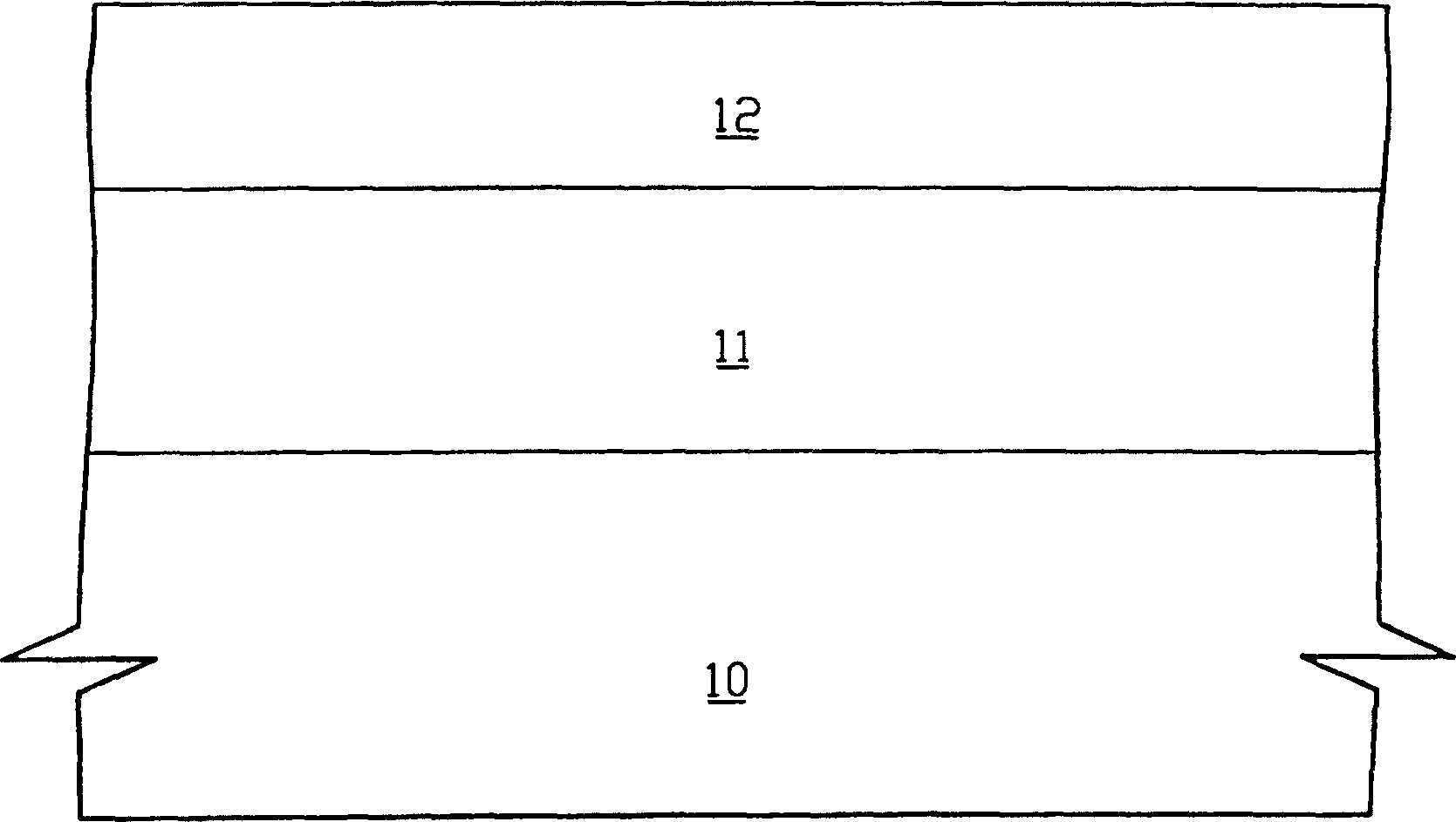
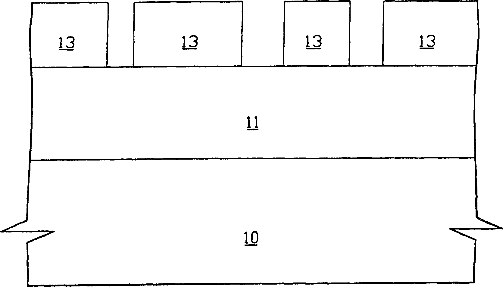
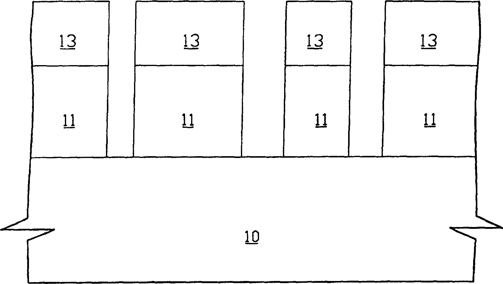
[0019] (3) Since the pattern transfer process is to transfer the pattern of the structure on the substrate to the substrate, it is possible to use photoresist and high etching resistance material to form a structure with a specific pattern instead of only using photoresist...


PUM


Abstract

A pattern transfer method, after the pattern photoresist is formed on the substrate, the pattern photoresist is subjected to a hardening process, and then the pattern of the pattern photoresist that has been cured is transferred to the substrate. Here, a common hardening process is a silicidation process, and only the top of the pattern photoresist can be hardened, or the top and sidewalls of the pattern photoresist can be hardened. Also, the height of the pattern photoresist and CD of the pattern photoresist can be reduced before performing the hardening process. Obviously, since the etching resistance of the hardened patterned photoresist is greater than that of the patterned photoresist material, the etching of the patterned photoresist in the pattern transfer process can be effectively reduced, thereby overcoming the problem of pattern distortion and overcoming When a thicker patterned photoresist is necessary to avoid the photoresist from being etched in the prior art, the critical dimension of the patterned photoresist is limited by the development capability and cannot be further reduced.

Description

(1) Technical field [0001] The invention relates to a method for pattern transfer. (2) Background technology [0002] The basic flow of a pattern transfer procedure using a lithography procedure is as follows: Figure 1A to Figure 1C As shown, a photoresist layer 12 is first formed on the layer 11 to be treated on the substrate 10, and then the photoresist layer 12 is patterned to form a pattern photoresist 13, and then an etching process is carried out on the layer 11 to be treated, so that the pattern photoresist The pattern of 13 is transferred to the layer 11 to be treated. Ideally, the pattern photoresist 13 will not be etched by the etching process at all, or at least the etched amount is negligibly small, so that the pattern of the pattern photoresist 13 can be accurately transferred to the layer 11 to be processed. [0003] The actual situation is that the etched amount of the pattern photoresist 13 is usually not negligible, especially when the thickness of the pat...

Claims


Application Information

Patent Timeline
Patent Type & Authority Patents(China)
IPC IPC(8): G03F7/00G03F7/16
Inventor 方震宇黄志贤林嘉祺黄瑞祯
Owner FUJIAN JINHUA INTEGRATED CIRCUIT CO LTD
Why Eureka
Try Eureka