Method for producing a transistor structure

A transistor, bipolar transistor technology, used in transistors, semiconductor/solid state device manufacturing, electric solid state devices, etc., to achieve low marginal capacitance, improved high current behavior, and reduced conduction effects

Inactive Publication Date: 2007-08-08
INFINEON TECH AG
View PDF8 Cites 0 Cited by
  • Summary
  • Abstract
  • Description
  • Claims
  • Application Information

AI Technical Summary

Problems solved by technology

However, such a method cannot form a clear junction between the different buried layers and the collector.

Method used


Image

  • Method for producing a transistor structure
  • Method for producing a transistor structure
  • Method for producing a transistor structure

Examples


Embodiment Construction

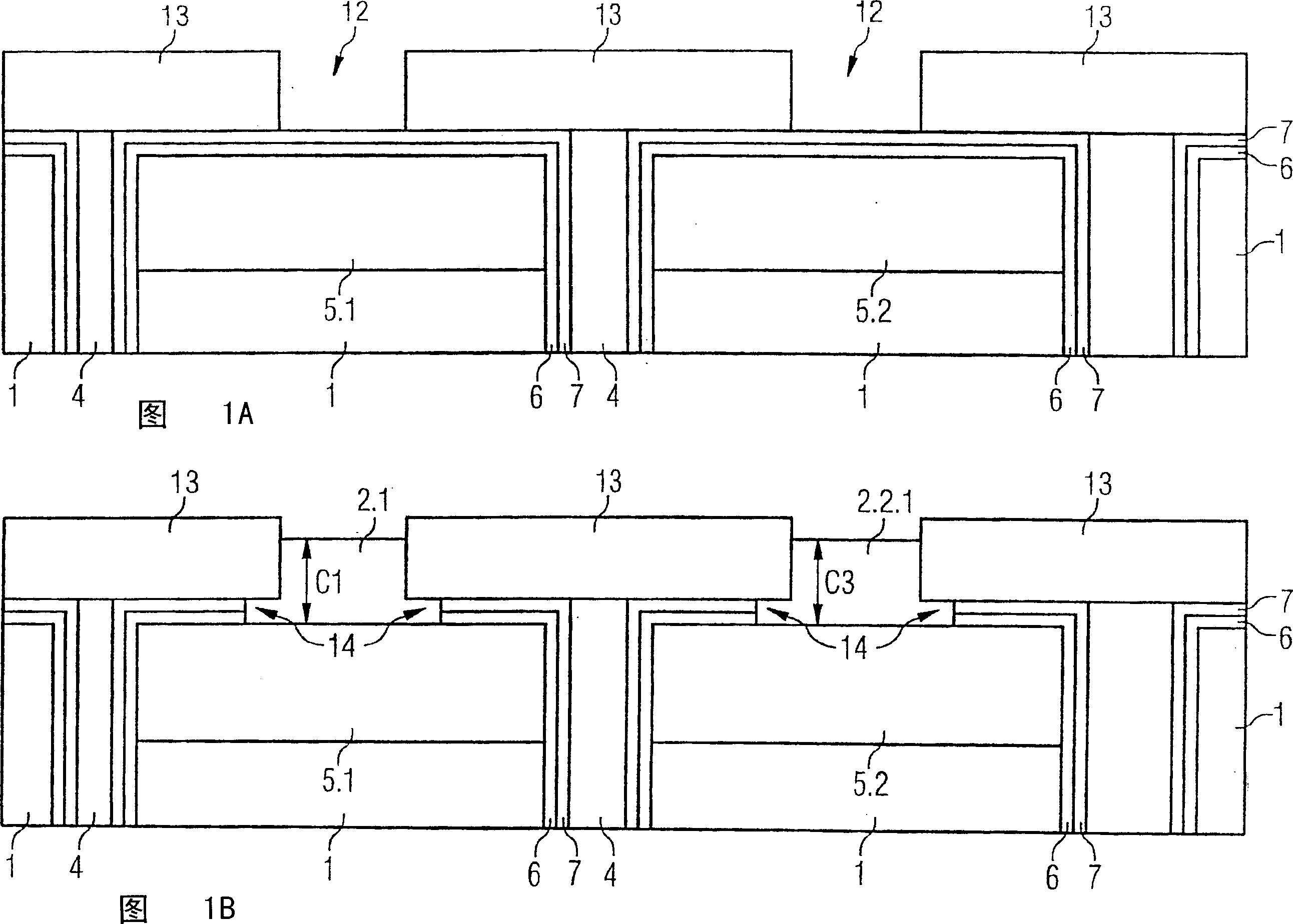
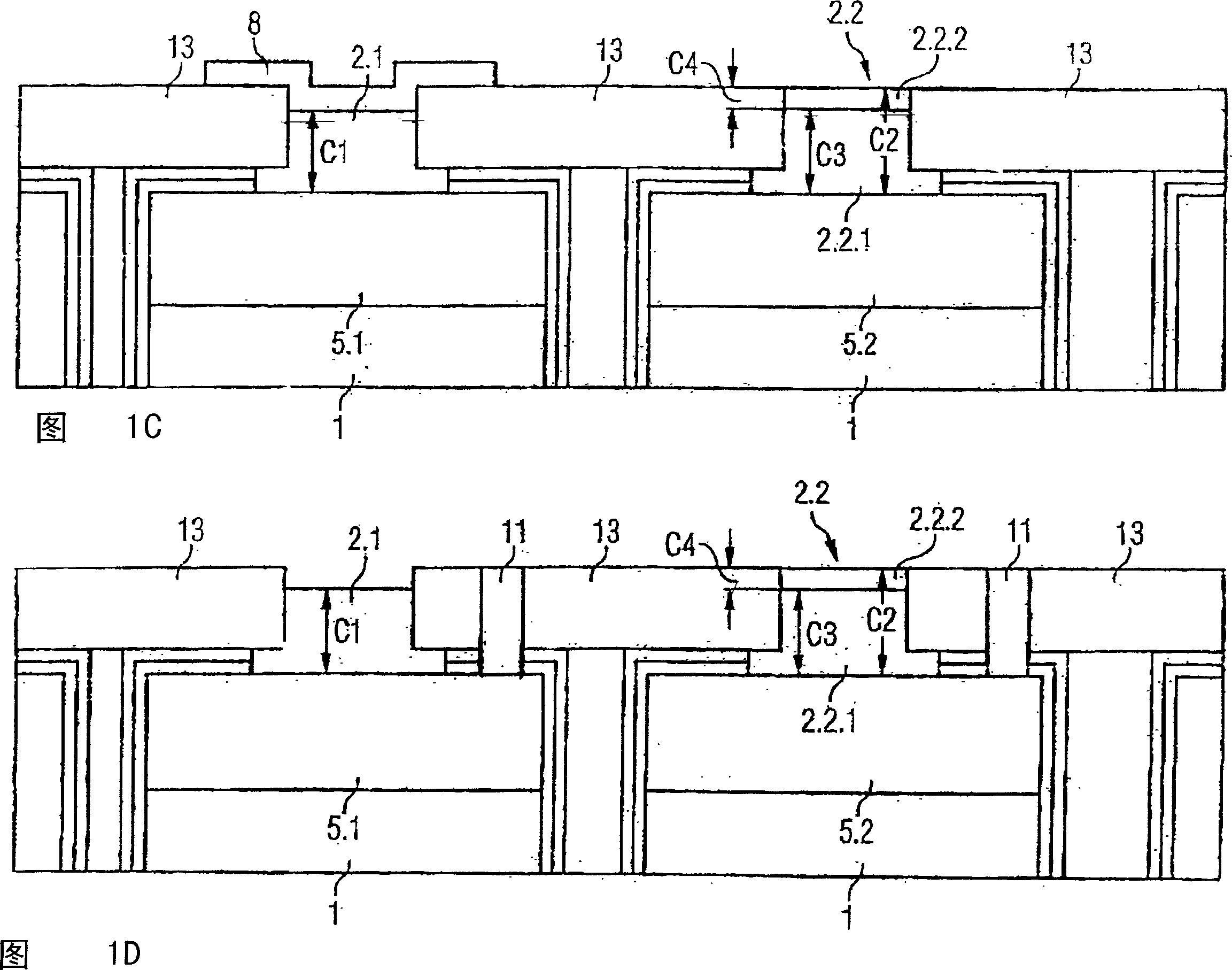
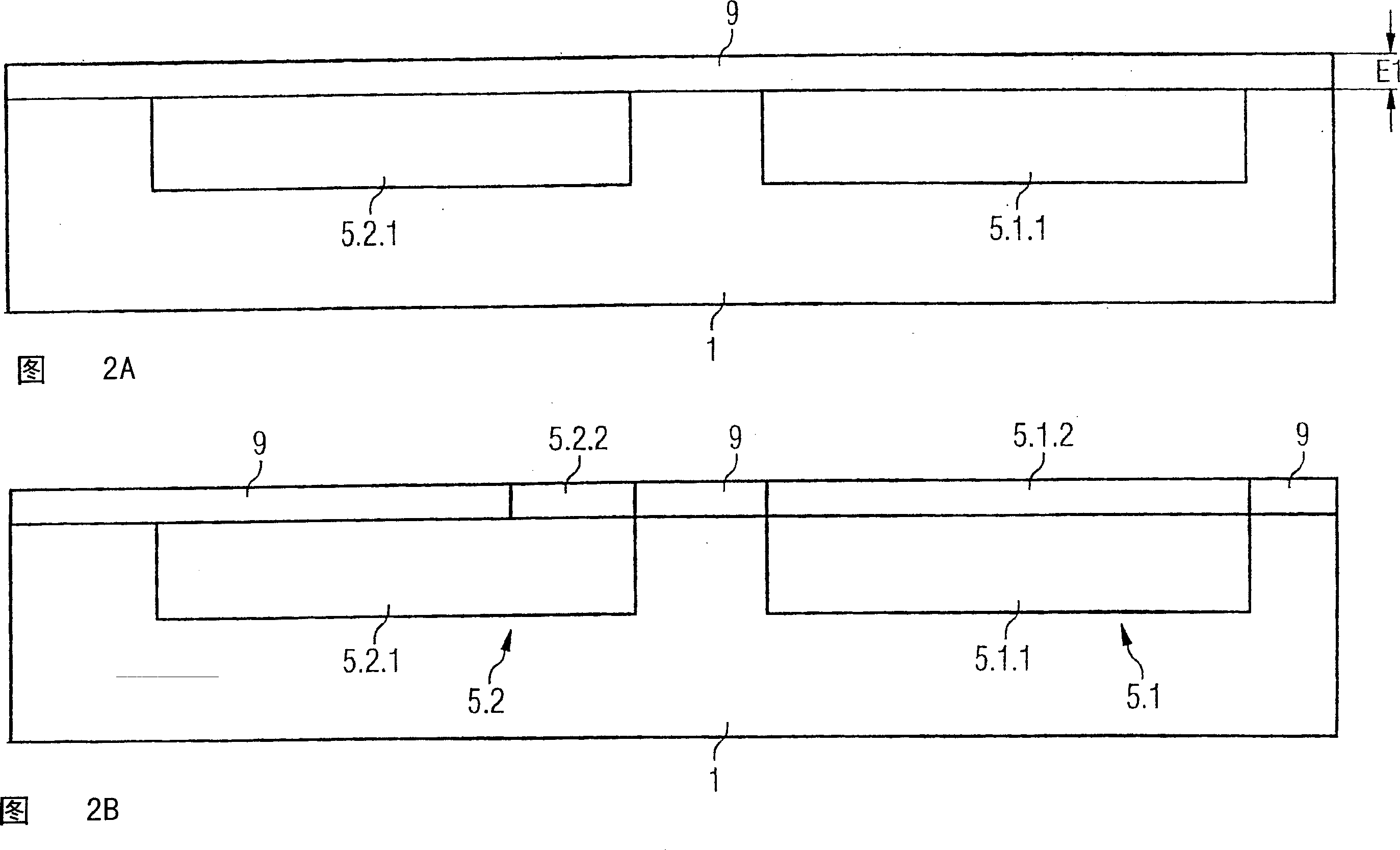
[0027] According to the first method of the present invention, a transistor structure for manufacturing two collector regions with different collector widths according to the present invention, as shown in the appended reference drawings FIGS. 1A to 1D , has been It is implemented by the technique of selective seeding.

[0028] The buried layer described in Figure 1A is, for example, n + Type-doped buried layers 5.1 and 5.2 have been introduced into the semiconductor substrate 1 and are insulated from each other by an insulating layer 4, here a deep trench 4 is formed. The semiconductor substrate 1 includes, for example, p-type doped single crystal silicon.

[0029] A first sublayer 6 and a second sublayer 7 are further provided and insulate the insulating layer 4 from the semiconductor substrate 1 and the buried layers 5.1 and 5.2. In this example, the second subsidiary layer 7 is adjacent to the insulating layer 4, and the first subsidiary layer 6 is adjacent to the second...


PUM


Abstract

The invention relates to a method for producing a transistor structure, comprised of at least one first and one second bipolar transistor with different collector widths. The invention is characterized in that all junctions between differently doped regions have a sharp interface. A first collector region (2.1) is suited for use in a high-frequency transistor having high limit frequencies fT, and a second collector region (2.2) is suited for use in a high-voltage transistor having increased breakdown voltages.

Description

technical field [0001] The present invention relates to a method of manufacturing a transistor structure comprising at least a first and a second bipolar transistor with different collector widths. Such a production method is known, for example, from German patent DE10044838C2. Background technique [0002] In bipolar transistors, the collector is usually terminated in a heavily doped buried layer. The buried layer is formed by subjecting the substrate to an ion introduction method at desired locations. After that, a lightly doped seed layer is applied and the base, emitter and collector wells are fabricated. A possible process sequence as described above is illustrated, for example, in Table 8.13 of "Technologie hochintegrierter Schaltungen", 2nd edition, pages 336-334 by D. Widmann, H. Mader, H. Friedrich, Springer Verlag. [0003] For integrated high-frequency circuits in the GHz range, it is usually preferred to combine a high-voltage transistor (HV transistor) with a...

Claims


Application Information

Patent Timeline
Patent Type & Authority Patents(China)
IPC IPC(8): H01L21/8222H01L27/082H01L29/08H01L21/331
CPCH01L27/0825H01L21/8222H01L29/0821H01L29/66272H01L21/18
Inventor J·贝克R·拉奇纳T·梅斯特H·沙弗M·塞克R·斯坦格
Owner INFINEON TECH AG
Why Eureka
Try Eureka