Wafer package structure and its base plate

A chip packaging and substrate technology, which is used in electrical components, electrical solid-state devices, circuits, etc.

Active Publication Date: 2007-08-08
CYNTEC
View PDF3 Cites 0 Cited by
  • Summary
  • Abstract
  • Description
  • Claims
  • Application Information

AI Technical Summary

Problems solved by technology

In order to solve the defects of the existing chip packaging structure and its substrate, the relevant manufacturers have tried their best to find a solution, but no suitable design has been developed for a long time. This is obviously a problem that the relevant industry is eager to solve

Method used


Image

  • Wafer package structure and its base plate
  • Wafer package structure and its base plate

Examples


Embodiment Construction

[0054] The specific structure, features and functions of the chip package structure and its substrate according to the present invention will be described in detail below with reference to the accompanying drawings and preferred embodiments.

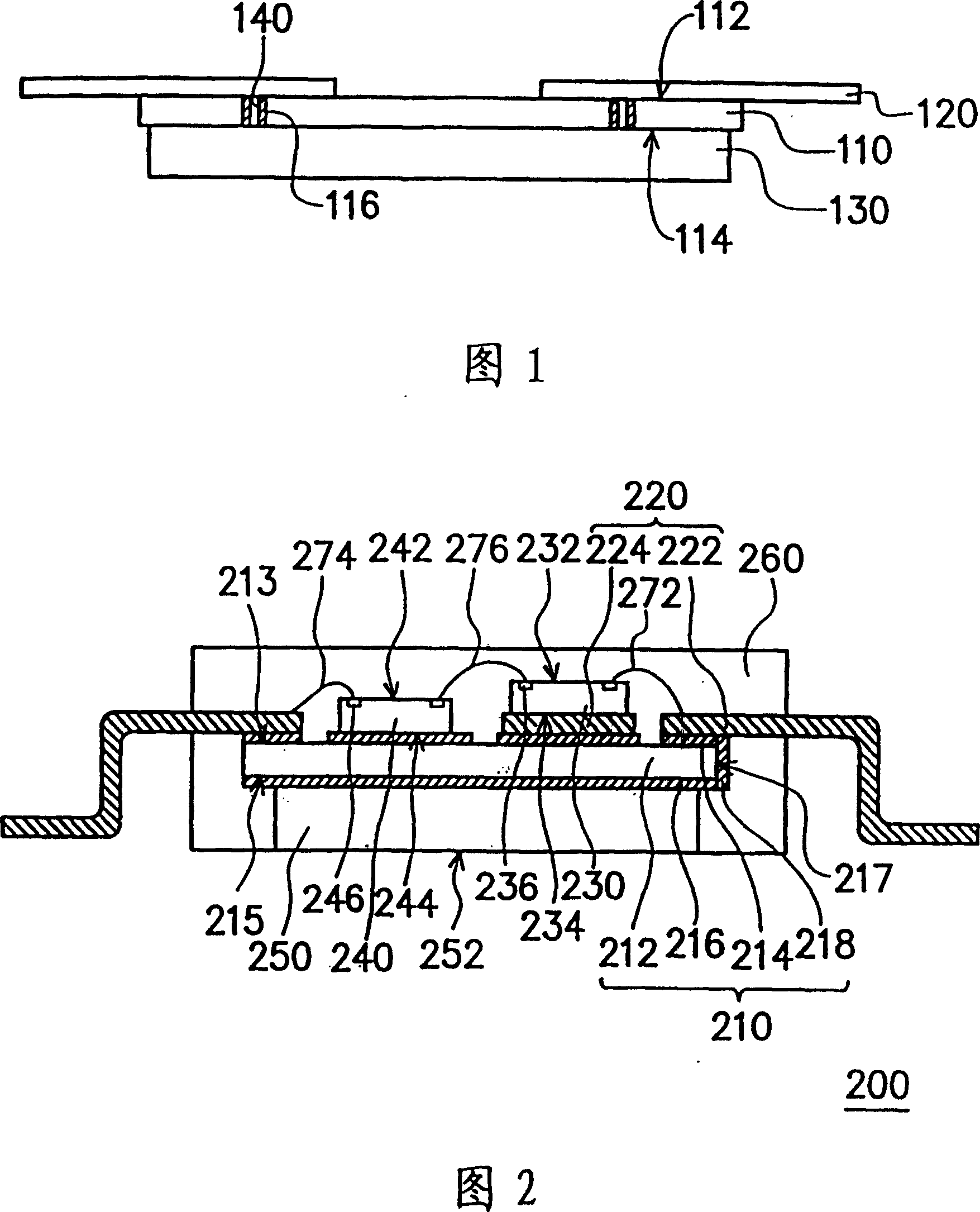
[0055] Please refer to FIG. 2 , which is a schematic cross-sectional view of a chip package structure of a high-power power module according to a preferred embodiment of the present invention. Generally speaking, the chip packaging structure 200 of the high-power power module includes a substrate 210 , a lead frame 220 , chips 230 , 240 , a heat sink 250 , a packaging material 260 and bonding wires 272 , 274 , 276 .

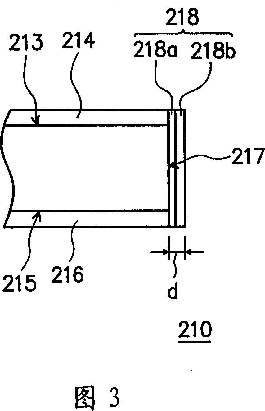
[0056] The substrate 210 is, for example, composed of an insulating layer 212, metal layers 214, 216 and a conductor 218, wherein the metal layer 214 is located on the upper surface 213 of the insulating layer 212, and the metal layer 216 is located on the lower surface 215 of the insulating layer 212. Above, the conductor ...


PUM


Abstract

This invention relates to a wafer packaging structure and its base plate including a base plate, a lead frame, a wafer, a lead, rediating fins and a packaging material, in which, the base plate has a first metal layer, a second metal layer and a conductor, the first metal layer is set at the first surface of the base plate, the second metal layer on its second surface the conductor on it side surface, the first metal layer is connected with the second metal layer via the electric conductor. The frame is on the first surface connected with the first metal layer, the wafer back is engaged in the frame or the first surface of the base plate, the lead is connected with the wafer and the lead frame, the radiating fin is placed at the second surface of the base plate electrically connected with the second metal layer, the packaging material wraps the wafer, lead and the frame.

Description

technical field [0001] The invention relates to a chip packaging structure and its substrate, in particular to a chip packaging structure and its substrate (CHIPPACKAGE AND SUBSTRATE) in which conductors are arranged on the side of the substrate to electrically connect the upper and lower surfaces of the substrate. Background technique [0002] In today's society of the information age, electronic products have become indispensable daily necessities for people, and the core of electronic products is chips, through which electronic products can perform logic operations or store data (data). Generally, after the power supply is output, it will pass through a high-power power supply module (module) to control the direction of the current and function as a switch. Since the high-power power supply module will bear the load of high current or high voltage transmitted from the power supply terminal, the high-power power supply module will generally generate a lot of heat, and the ...

Claims


Application Information

Patent Timeline
Patent Type & Authority Patents(China)
IPC IPC(8): H01L23/12H01L23/48H01L23/34H01L23/28
CPCH01L2924/0002H01L2224/48137H01L2224/48091H01L2224/73265H01L2224/48247H01L2924/00014
Inventor 陈大容林哲弘廖庆雄徐振杰
Owner CYNTEC
Why Eureka
Try Eureka