

Method and system for cleaning semiconductor wafer
A cleaning system and semiconductor technology, which is applied in semiconductor/solid-state device manufacturing, electrical components, circuits, etc., can solve the problems of mechanical component performance degradation, inefficiency, and safety, so as to improve safety, increase efficiency, and reduce waste Effect
- Summary
- Abstract
- Description
- Claims
- Application Information
AI Technical Summary
Problems solved by technology
Method used
Image

Examples
Embodiment Construction
[0031] A method and system for cleaning the surface of a semiconductor wafer are disclosed herein. In the following description, numerous specific details are set forth in order to provide a thorough understanding of the present invention. It will be appreciated, however, to one of ordinary skill in the art that the present invention may be practiced without some or all of these specific details. Additionally, well-known program operations have not been described in detail so as not to unnecessarily obscure the present invention.
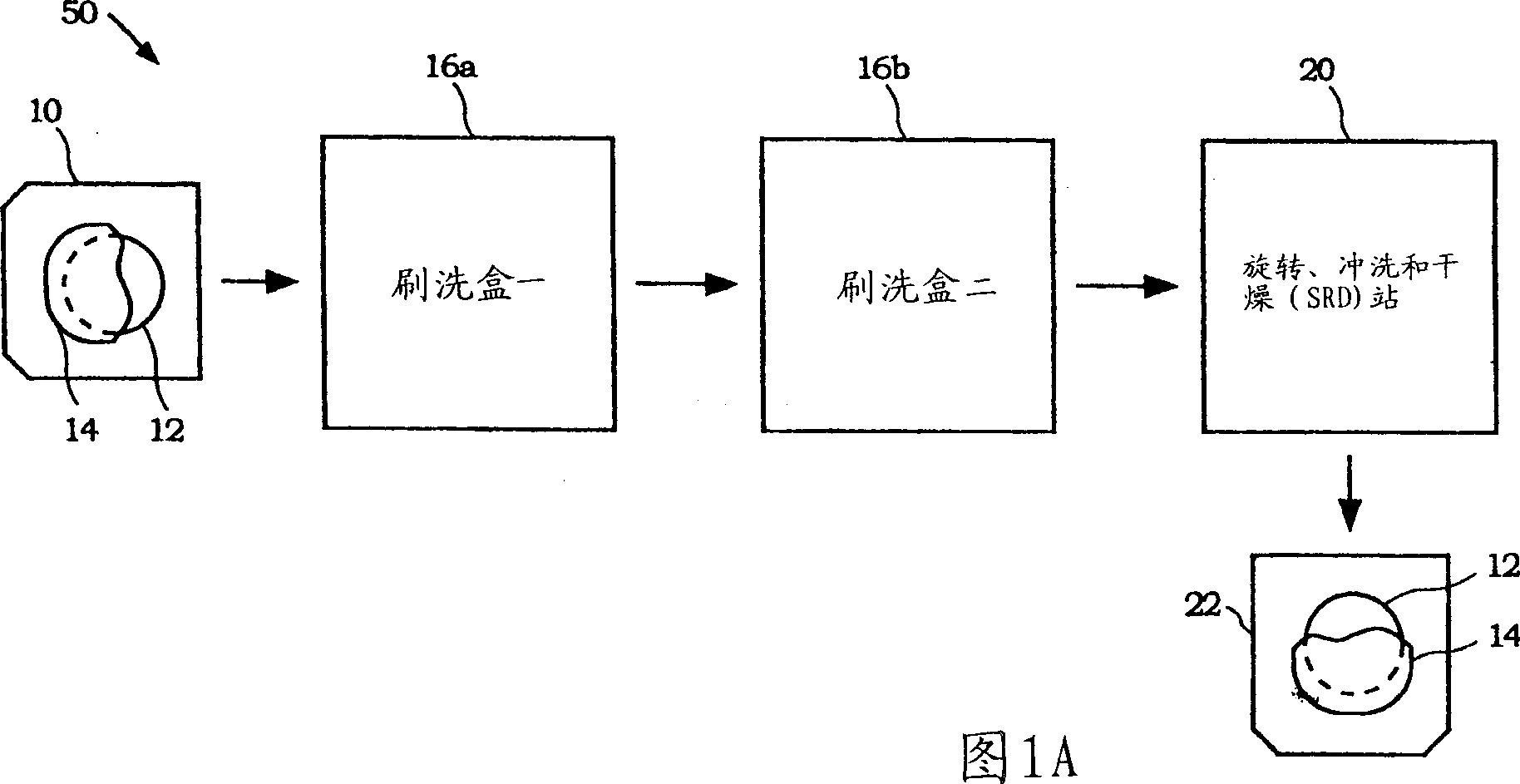
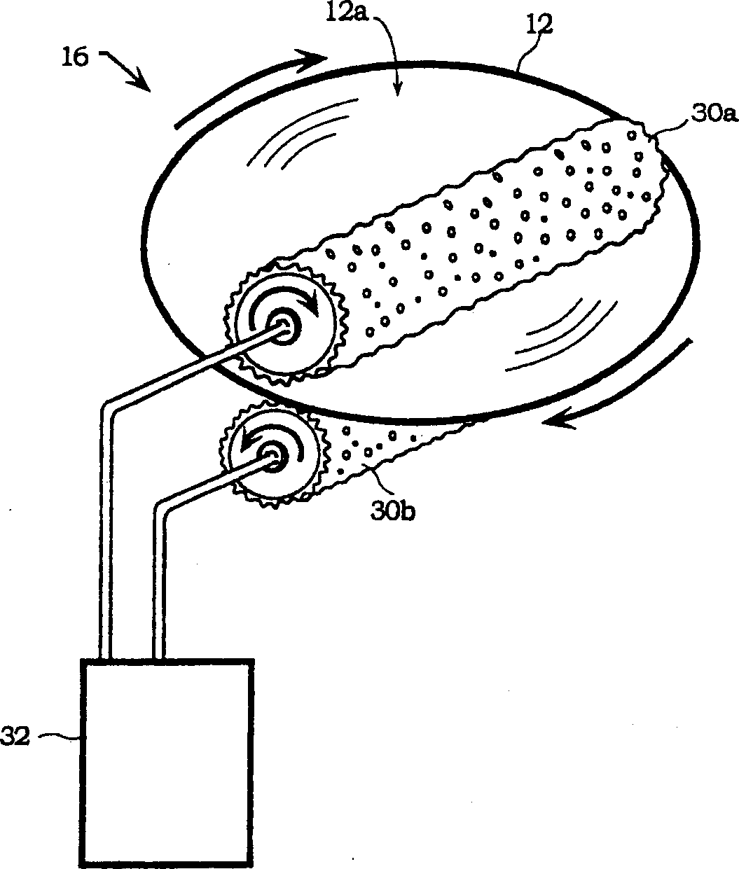
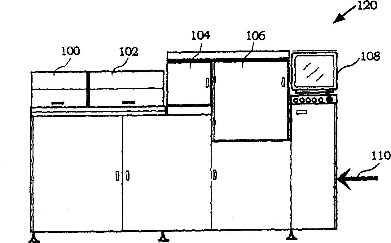
[0032] Figure 2A with 2B Side and top views of cleaning system 120 are shown, respectively. The cleaning system 120 basically includes an input station 100 into which a plurality of wafers are inserted to pass through the system for cleaning. Once the wafer is inserted into the input station 100, a wafer is taken from the input station 100 and moved to a brush box one 102a where the wafer is selected before being moved to the brush box two 102b...
PUM
 Abstract
Description
Claims
Application Information