

Connecting tape for semiconductor chip loading, carrier and package for semiconductor chip
A chip carrier and semiconductor technology, applied in the fields of semiconductor devices, semiconductor/solid-state device manufacturing, semiconductor/solid-state device components, etc., can solve the problems of low yield, waste of bonding sheets, waste of cost, etc., to improve yield, prevent The effect of using waste and reducing costs
- Summary
- Abstract
- Description
- Claims
- Application Information
AI Technical Summary
Problems solved by technology
Method used
Image

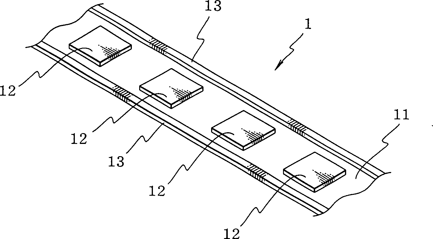
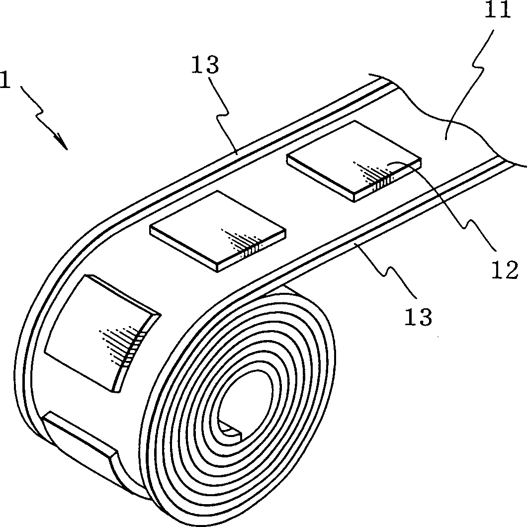
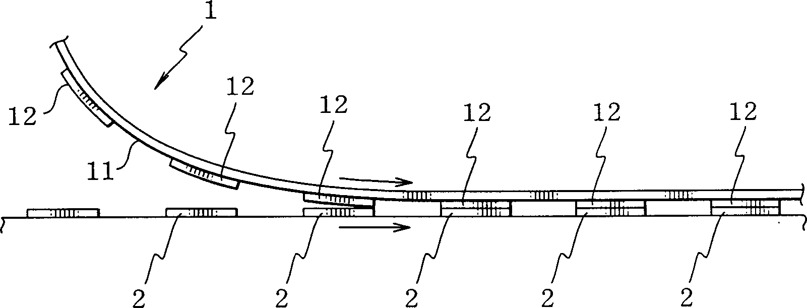
Examples
Embodiment 1
[0125] Production of bonding tape for mounting semiconductor chips (adhesive: composition a)
[0126] 55 parts by weight of butyl acrylate, 10 parts by weight of methyl methacrylate, 20 parts by weight of glycidyl methacrylate, and 15 parts by weight of 2-hydroxyethyl acrylate were copolymerized to prepare a copolymer having a weight average molecular weight of 900,000.
[0127] Mix 10 parts by weight of the above-mentioned copolymer, 24 parts by weight of liquid bisphenol A type epoxy resin (EPICO-TO 828 manufactured by Yuka Shell Epoxy Resin Co., Ltd.), 24 parts by weight of o-cresol novolac type epoxy resin (Nippon Kasaku Co., Ltd. EOCN-104S) 10 parts by weight, 0.05 parts by weight of γ-glycidoxypropyltrimethoxysilane as a coupling agent, 1.5 parts by weight of cyanoguanidine as a thermally active latent curing agent, 2-phenyl - 4,5-hydroxymethylimidazole, 5 parts by weight of urethane acrylate oligomer (Seikabi-M 14-29B manufactured by Dainichi Seika Co., Ltd.) as a pho...
Embodiment 2
[0132] Manufacture of bonding tape for semiconductor chip loading (adhesive: polyimide resin)
[0133] Composition a in Example 1 was replaced with a tetrahydrofuran solution (solid content: 20% by weight) of thermoplastic polyimide (UPITITO UPA-N221 manufactured by Ube Industries, Ltd.) to release one side with a silicone resin The polyethylene naphthalate (PEN) film (surface tension: 34dyn / cm) of processing replaces the PET film that one side is carried out release treatment with silicone resin in embodiment 1, except thermoplastic polyimide The drying conditions were set at 90° C. and 5 minutes, and the rest were the same as in Example 1 to prepare a bonding tape for semiconductor chip loading.
Embodiment 3
[0135] Manufacture of bonding tape for mounting semiconductor chips (adhesive: epoxy-based resin composition)
[0136] Mix 40 parts by weight of high-molecular-weight bisphenol-type epoxy resin (EPICO-TO 1010, manufactured by Yuka Shell Epoxy Resin Co., Ltd.), and 20 parts by weight of multifunctional cresol novolak-type epoxy resin (EOCN-4600, manufactured by Nippon Kayaku Co., Ltd.) Parts by weight, 1.5 parts by weight of 2-phenyl-4,5-hydroxymethylimidazole as a thermally active latent curing agent and 0.1 parts by weight of γ-glycidoxypropyltrimethoxysilane, as epoxy Resin bonding agent.
[0137] Except that the above-mentioned epoxy resin adhesive was used instead of the composition a in Example 1, the rest were the same as in Example 1, and a bonding tape for semiconductor chip loading was produced.
PUM
| Property | Measurement | Unit |
|---|---|---|
| melting point | aaaaa | aaaaa |
| thickness | aaaaa | aaaaa |
| wavelength | aaaaa | aaaaa |
Abstract
Description
Claims
Application Information