Non-linear signal processor
A nonlinear and processor technology, applied in the field of signal processing systems that process signals nonlinearly, can solve problems such as power supply voltage difference and ground potential difference
- Summary
- Abstract
- Description
- Claims
- Application Information
AI Technical Summary
Problems solved by technology
Method used
Image

Examples
Embodiment Construction
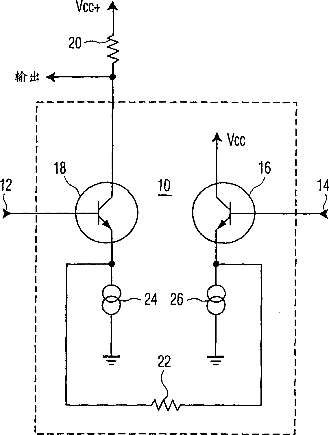
[0020] The present invention is described below in the context of an exemplary embodiment comprising a television signal processing system. However, the invention can be applied to other types of signal processing systems.
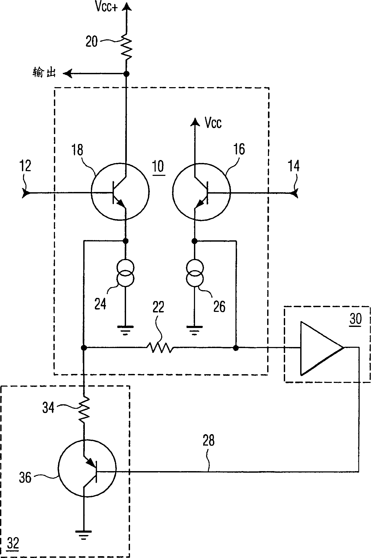
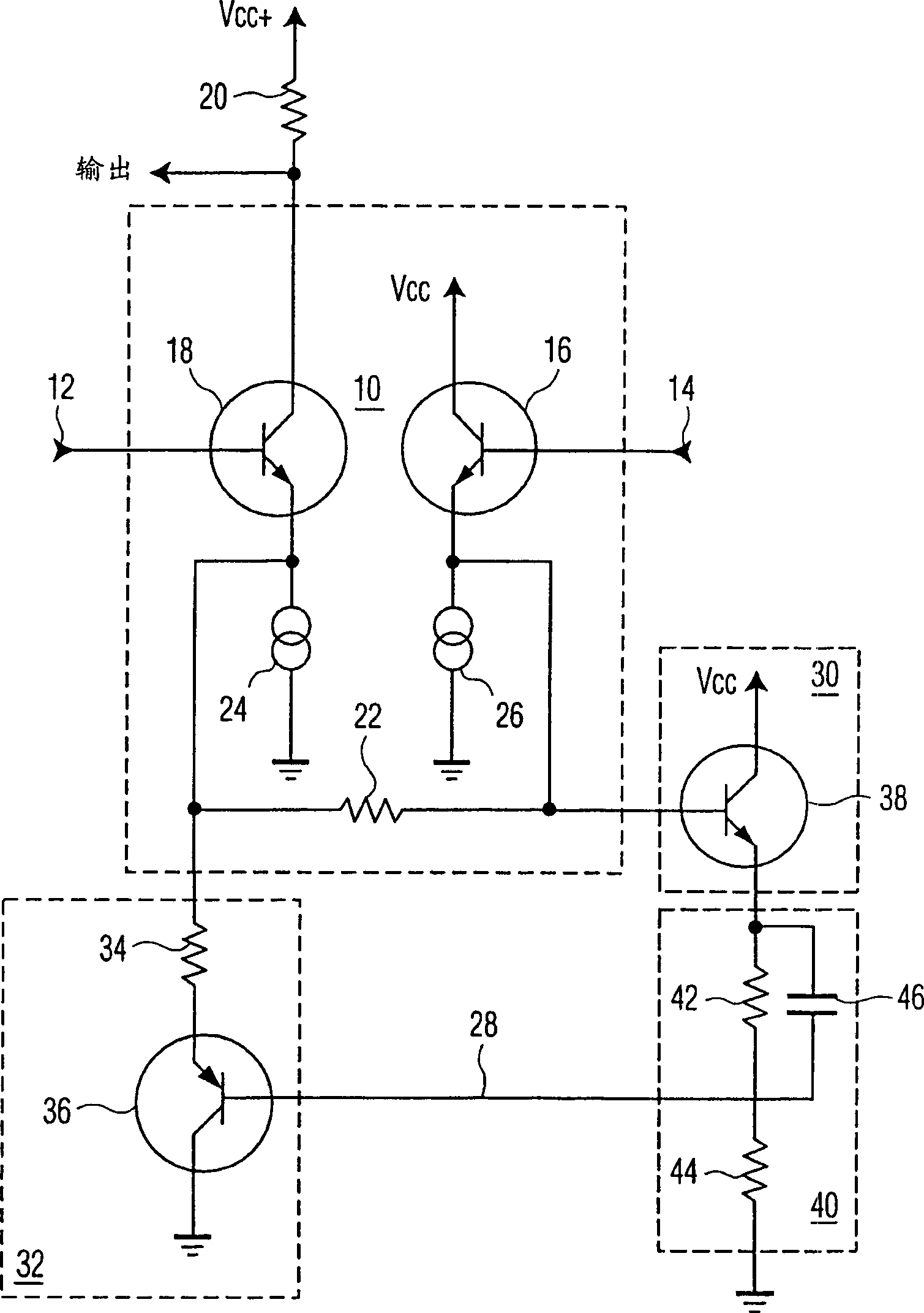
[0021] A signal processing system such as a television signal processing system typically includes means for amplifying a voltage signal, for example, either a demodulated luminance signal or a component color signal. It is often desirable to provide the amplifier with non-linear gain characteristics. Such as figure 1 As shown, this is often the case, ie, using a differential amplifier 10 where one input 12 to the amplifier 10 contains the desired time-varying signal and the other input 14 provides a common mode bias for the amplifier 10 . It is also common for time-varying common mode components to be present on each of the two input signals. exist figure 1 A common mode bias 14 is applied to the base of transistor 16 in the circuit of , and a time-va...
PUM
 Abstract
Description
Claims
Application Information
 - R&D
- Intellectual Property
- Life Sciences
- Materials
- Tech Scout
- Unparalleled Data Quality
- Higher Quality Content
- 60% Fewer Hallucinations
Browse by: Latest US Patents, China's latest patents, Technical Efficacy Thesaurus, Application Domain, Technology Topic, Popular Technical Reports.
© 2025 PatSnap. All rights reserved.Legal|Privacy policy|Modern Slavery Act Transparency Statement|Sitemap|About US| Contact US: help@patsnap.com