Check patentability & draft patents in minutes with Patsnap Eureka AI!

Optical proximity effect correcting method

A technology of optical proximity effect and transparent film, which is applied in the fields of optics, components for photomechanical processing, photomechanical equipment, etc., and can solve problems such as difficulty in making and correcting photomasks

Inactive Publication Date: 2003-03-19
UNITED MICROELECTRONICS CORP
View PDF0 Cites 7 Cited by
  • Summary
  • Abstract
  • Description
  • Claims
  • Application Information

AI Technical Summary

Problems solved by technology

Mask fabrication and correction has become more and more difficult since the large data size caused by optical proximity correction

Method used


Image

  • Optical proximity effect correcting method
  • Optical proximity effect correcting method
  • Optical proximity effect correcting method

Examples


Embodiment Construction

[0017] The method of the present invention can be widely applied to many semiconductor designs, and can be made using many different semiconductor materials. When the present invention describes the method of the present invention with a preferred embodiment, those who are familiar with this field should have It is recognized that many steps can be changed, and materials and impurities can also be replaced, and these general replacements undoubtedly do not depart from the spirit and scope of the present invention.

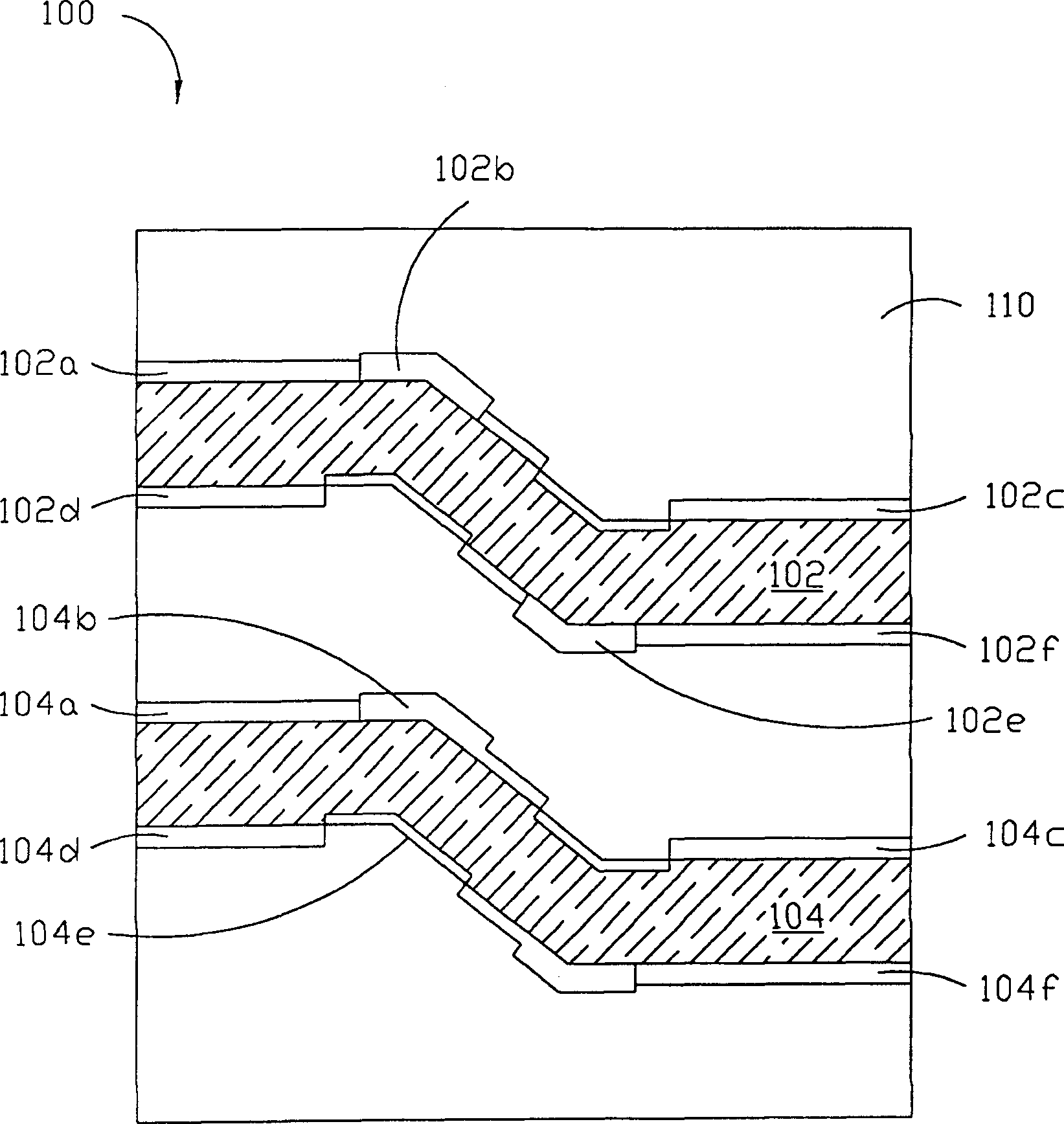
[0018] Secondly, the present invention is described in detail with schematic diagrams as follows. When describing the embodiments of the present invention in detail, the cross-sectional view showing the semiconductor structure will not be partially enlarged according to the general scale in the semiconductor manufacturing process for the convenience of explanation, but it should not be used as a limited definition. Know. In addition, in actual production, the three...


PUM


Abstract

The optical proximity effect correcting method includes providing one transparent plate, forming opaque film on the plate in polygon, and increasing at least one convex angle to one side of the polygon.

Description

(1) Technical field [0001] The invention relates to a lithographic equipment component, in particular to a method for correcting optical proximity effect. (2) Background technology [0002] The dimensions of the smallest features of integrated circuits have been shrinking continuously over the years. Concomitantly associated with scaling down is the difficulty in manufacturing integrated circuits on various process constraints. The main limitation that has been shown in the field of fabrication technology is photolithography. [0003] To selectively protect areas of the wafer (such as the substrate, polysilicon, or dielectric), lithography involves coating a photoresist on the silicon wafer, selectively exposing areas to form an illumination pattern, and then The exposed photoresist is developed. [0004] An integral part of a lithography device is a mask that includes a pattern of features corresponding to a layer of the integrated circuit design. Such reticles generall...

Claims


Application Information

Patent Timeline
IPC IPC(8): G03F1/00G03F1/36G03F7/20
CPCG03F1/144G03F7/70441G03F1/36
Inventor 谢昌志林本立陈明瑞
Owner UNITED MICROELECTRONICS CORP
Features
  • R&D
  • Intellectual Property
  • Life Sciences
  • Materials
  • Tech Scout
  • Unparalleled Data Quality
  • Higher Quality Content
  • 60% Fewer Hallucinations
Learn More