Control device for zero-voltage conversion step-up power factor correcting circuit

A power factor correction and control device technology, applied in output power conversion devices, high-efficiency power electronic conversion, electrical components, etc., can solve problems such as AC input voltage peak value can not be too high, inductance L has noise, oscillation and other problems

Inactive Publication Date: 2003-06-11
ZTE CORP
View PDF0 Cites 3 Cited by
  • Summary
  • Abstract
  • Description
  • Claims
  • Application Information

AI Technical Summary

Problems solved by technology

[0016] The technical problem to be solved by the present invention is to overcome the deviation existing in the control of the main control chip of the ZVT Boost PFC circuit in the prior art, resulting in the shortcoming that the peak v

Method used


Image

  • Control device for zero-voltage conversion step-up power factor correcting circuit
  • Control device for zero-voltage conversion step-up power factor correcting circuit
  • Control device for zero-voltage conversion step-up power factor correcting circuit

Examples


Embodiment Construction

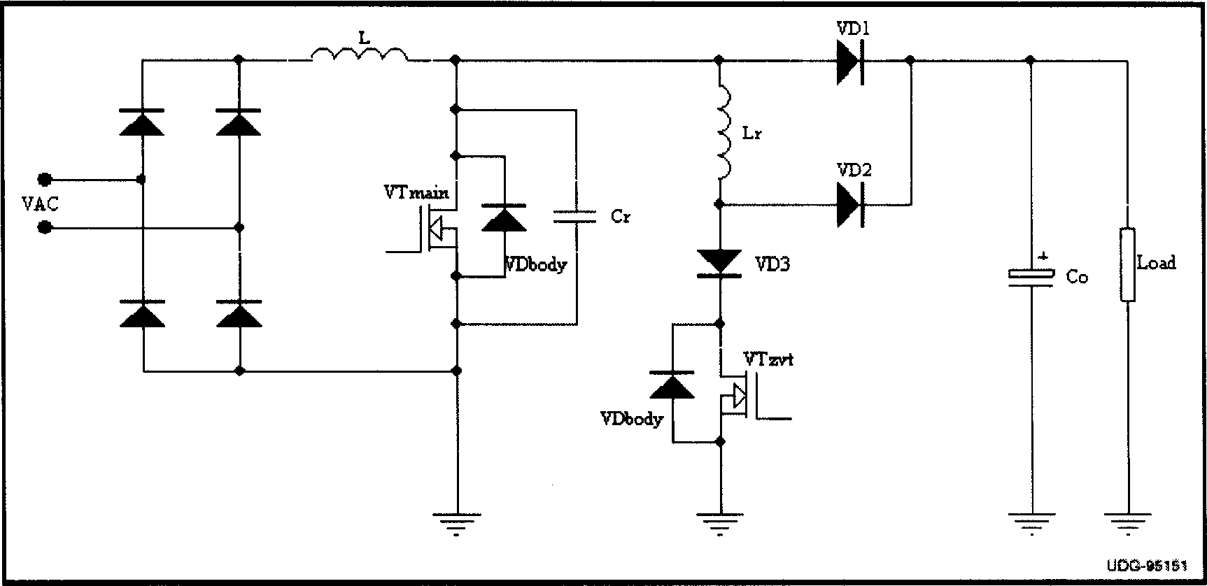
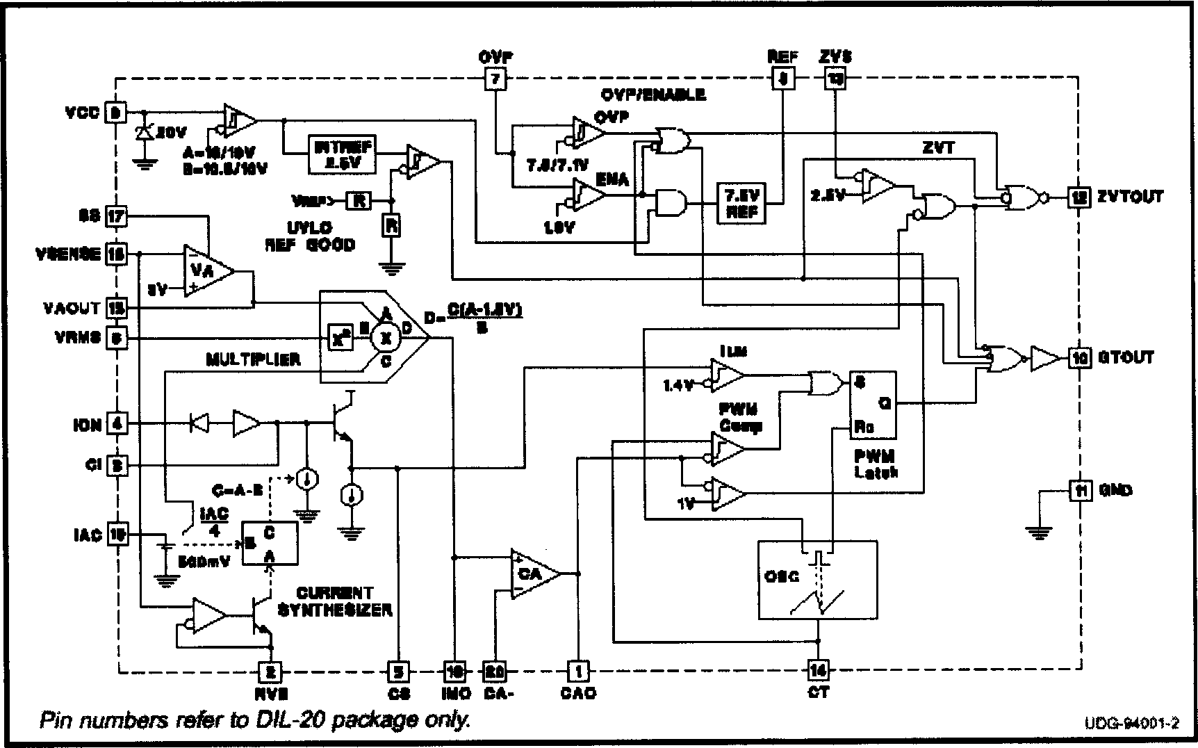
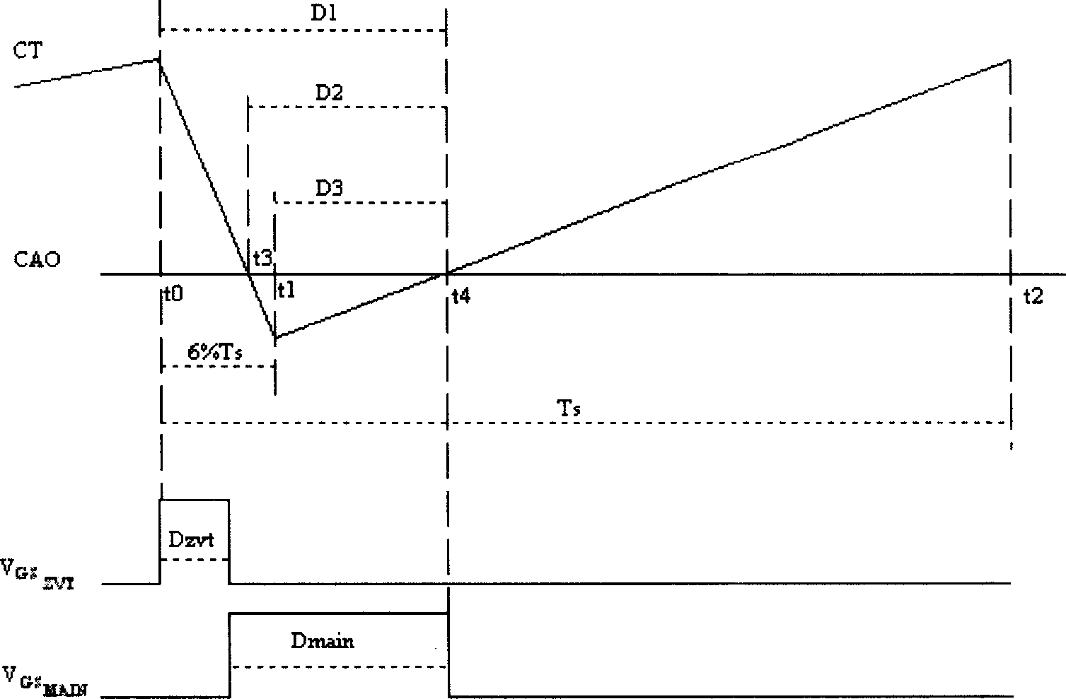
[0024] figure 1 , figure 2 , image 3 Corresponding descriptions have been given in the background art section.

[0025] Figure 4 For realizing the functional block diagram of the present invention: supervisory drain-source terminal voltage detection circuit 101, V DS MAIN is the main drain-source terminal voltage, ZVS is its detection signal, when V DS MAIN When it is low, ZVS is low level, otherwise it is high level, and the conversion value of high and low levels is determined by the logic circuit characteristics in the main and auxiliary pipe drive pulse distribution circuit 103; the PWM comparator circuit 102 generates a DRV with a duty cycle of D2 Signal; the main and auxiliary pipe drive pulse distribution circuit 103 is a circuit for realizing the construction of the auxiliary pipe drive signal VTzvt and the main pipe drive signal VTmain from the DRV, and satisfies the following three conditions:

[0026] 1. Auxiliary pipe drive signal: V GSZVT =DRV·ZVS,

[00...


PUM


Abstract

A control device for zero-voltage conversion step-up power factor correcting circuit includes main source/drain voltage detection circuit, PWM comparator circuit and main assistant drive pulse distribution circuit; after detected by its detecting circuit, the VDSMAIN outputs ZVS, when VDSMAIN is low, ZVS is at low or high level, conversion of which is decided by logic circuit properties in main assistance drive pulse distribution circuit;PWM comparator circuit generates DRV signal with duty ratio of D2 and the pulse distribution circuit realizes making up assist drive signal VTzvt and main drive signal VTmain, so to satisfy sum of VGSZVT=DRV.ZVS and VGSMain=DRV.ZVS:VGSZVT+VGsmain=DRV.

Description

technical field [0001] This description relates to the control circuit of the zero-voltage conversion boost power factor correction (ZVT Boost PFC) circuit, and specifically involves the distribution control of the duty cycle of the main and auxiliary pipe drive pulses. Background technique [0002] Increasing the switching frequency can reduce the size and weight of magnetic devices, so it has always been one of the important directions for the development of power electronic switching technology. However, at high switching frequencies, the EMI problem when the main diode of the BoostPFC circuit is turned off and the main switching tube The switching loss problem has become more serious, and the hard switching technology is obviously not suitable, so the ZVT Boost PFC circuit and its control technology are proposed, and the United States Unitrode Company has developed a special control chip UC3855A / B for this circuit. [0003] figure 1 It is the schematic diagram of the ZV...

Claims


Application Information

Patent Timeline
IPC IPC(8): H02M1/08
CPCY02B70/1491Y02B70/10
Inventor 罗勇王毅徐波
Owner ZTE CORP
Why Eureka
Try Eureka