

Liquid crystal light shutter, optical printing head and method for producing lquid crystal light shutter
A liquid crystal and door panel technology, applied in the field of optical print heads, can solve the problems of increased manufacturing processes, waste of precious metal film 13, and increased manufacturing costs
- Summary
- Abstract
- Description
- Claims
- Application Information
AI Technical Summary
Problems solved by technology
Method used
Image

Examples
Embodiment 1
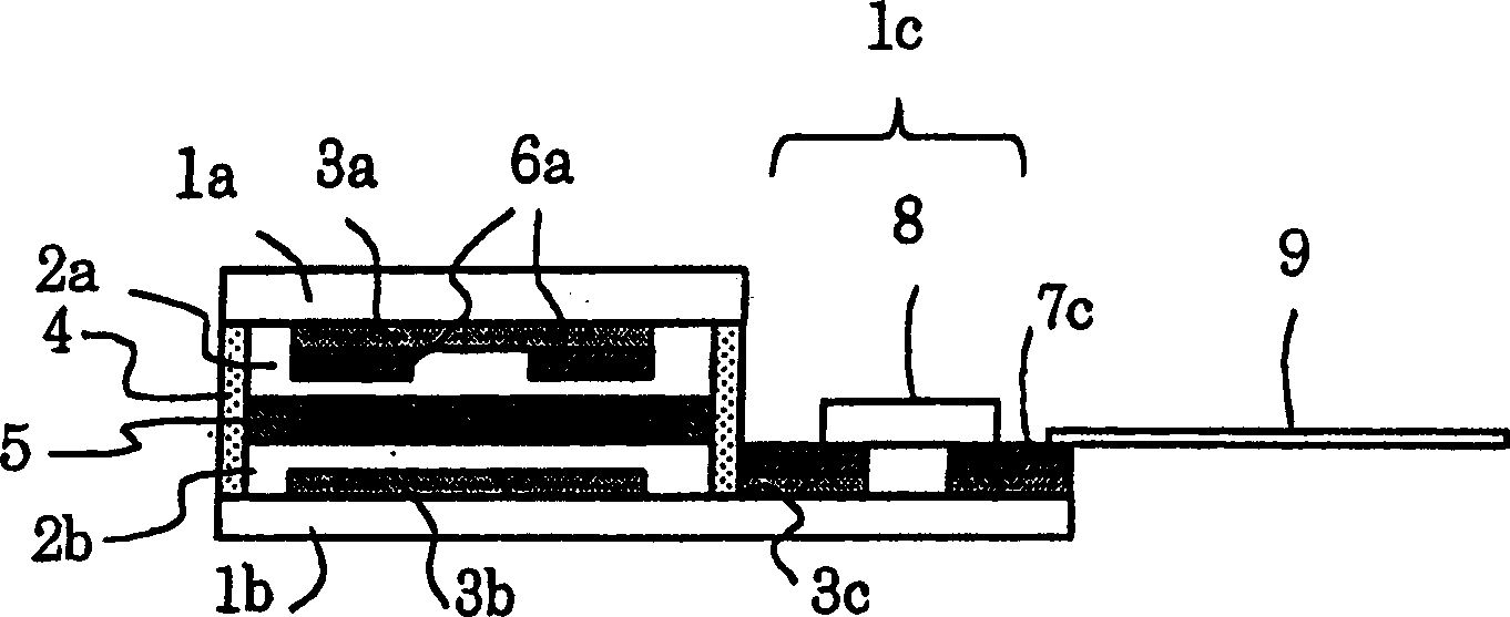
[0088] figure 1 It is a cross-sectional view showing the structure of a COG (Chip On Glass: Chip On Glass) type liquid crystal light gate panel in which a driver IC is mounted in Embodiment 1 of the present invention.
[0089] exist figure 1 Middle 1a is the upper side glass substrate, on which a common electrode 3a made of ITO (Indium Tin Oxide: Indium Tin Oxide) and a gold film light-shielding film 6a made of gold film are formed. 1b is a lower glass substrate on which a pixel electrode 3b made of ITO is formed. 2a is the upper side alignment film, 2b is the lower side alignment film, the liquid crystal 5 is sealed in the liquid crystal cell formed by bonding the upper side glass substrate 1a and the lower side glass substrate 1b with the sealing material 4.
[0090] An image information signal (input signal) is input to the pixel electrode 3b, and the liquid crystal 5 is driven according to the image information signal.
[0091] Liquid crystal drive IC8 is installed on...
Embodiment 2
[0112] Use below Figure 4 Example 2 will be described.
[0113] Figure 4 A graph showing the relationship between the film thickness of the gold film light-shielding film 6a obtained through experiments and the light transmittance, R represents red light (center wavelength 650nm), G represents green light (center wavelength 550nm), and B represents blue light. The color lights (center wavelength 470nm) represent the proportion of light of each wavelength passing through the gold film light-shielding film 6a (except for the opening). Depend on Figure 4 It can be seen that if the thickness of the gold film is more than 0.28 μm, the transmittance in the entire wavelength region is less than 0.2%, and the light leakage from the gold film light-shielding film 6a can be suppressed. The method for increasing the thickness of the gold film shading film 6a includes in image 3 Repeat the method of coating (more than 2 times) organic gold glue in the process b. The other steps a...
Embodiment 3
[0117] Use below Figure 5 and Image 6 Example 3 will be described.
[0118] Figure 5 (a) is a perspective view showing an exploded structure of the print head of Embodiment 3 that adopts the liquid crystal light gate plate in Embodiments 1 and 2; Figure 5 (b) is to represent the top view of the top (see A direction among the figures) of the liquid crystal light gate plate among the embodiment 1,2, and Image 6 is a detailed cross-sectional view showing the structure of the print head.
[0119] The print head is configured such that the light source part 21 having the light source substrate 20 loaded with light sources, that is, a plurality of LEDs 19, is in contact with or close to the upper glass on which the gold film light-shielding film 6a on the liquid crystal light gate plate 18 shown in Embodiment 2 is formed. Substrate 1a side ( Figure 5 , Image 6 in the direction of arrow A).
[0120] Image 6 Among them, the light source unit 21 is composed of a light g...
PUM
| Property | Measurement | Unit |
|---|---|---|
| thickness | aaaaa | aaaaa |
Abstract
Description
Claims
Application Information