

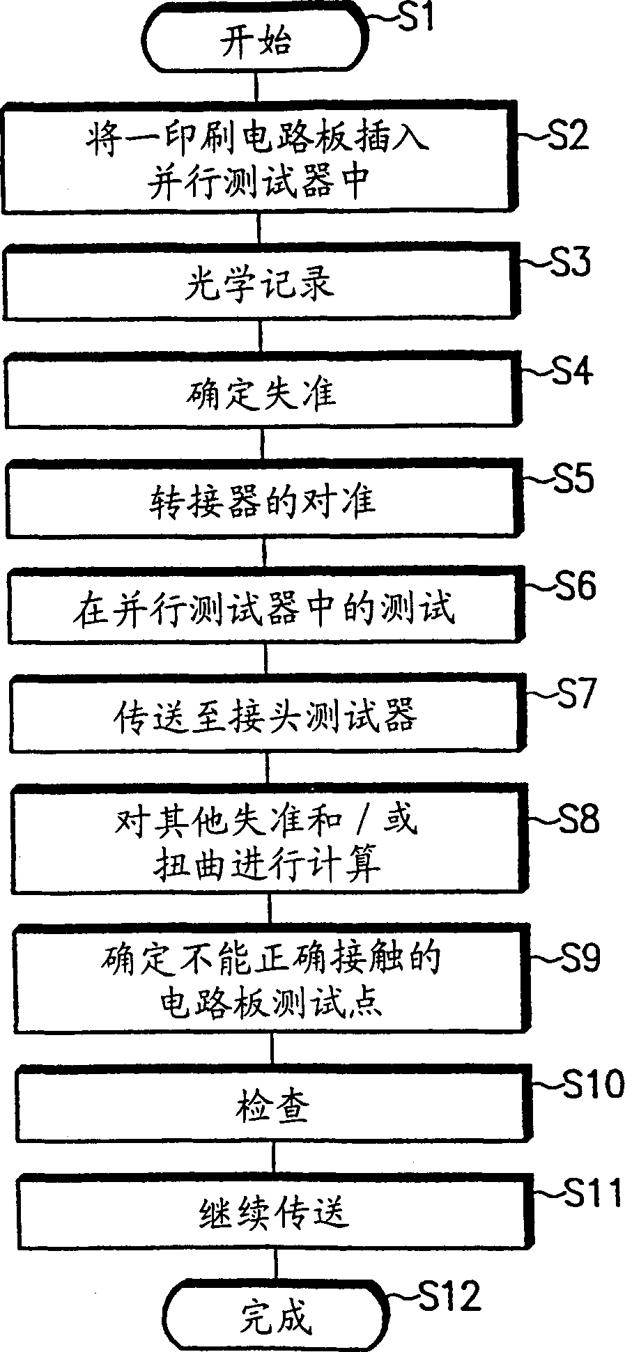
Method and device for testing printed circuit boards with a parallel tester
A printed circuit board, test printing technology, applied in the directions of printed circuit, printed circuit manufacturing, printed circuit testing, etc., can solve problems such as wrong measurement, slow connector tester, and test probes that cannot be close to each other.
- Summary
- Abstract
- Description
- Claims
- Application Information
AI Technical Summary
Problems solved by technology
Method used
Image

Examples
Embodiment Construction
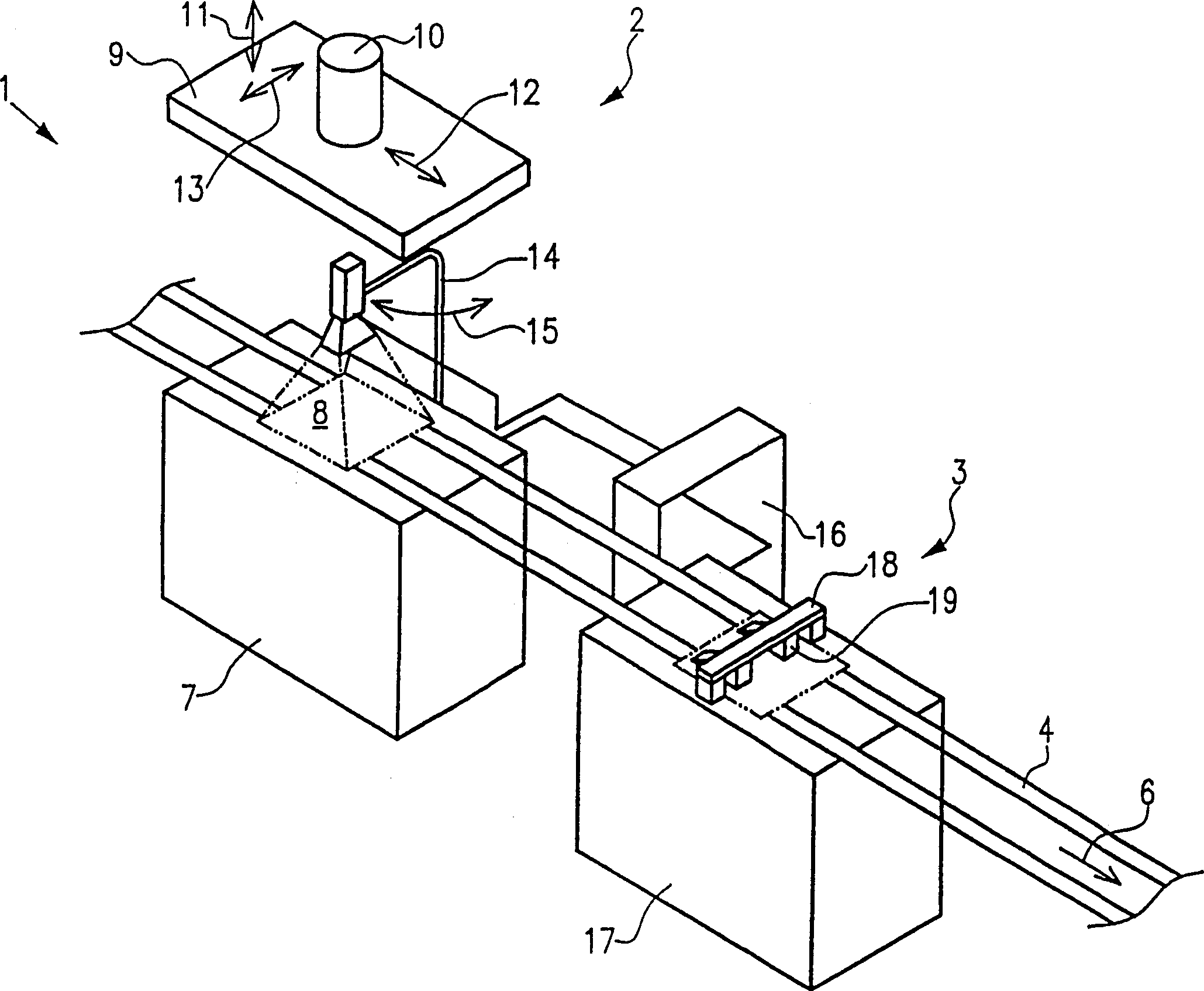
[0050] figure 1 is shown schematically an apparatus according to the invention for testing printed circuit boards. The device 1 has a parallel tester 2 and a joint tester 3 . The parallel tester 2 and the joint tester 3 are connected by a conveyor 4 , which is formed by two conveyor belts 5 in this embodiment. With the conveyor 4, the printed circuit boards to be tested can be transferred in the transfer direction 6 from a substantially known but not shown separation station to the parallel tester 2 and from the parallel tester 2 to the joint tester 3, and From the splice tester 3 it is conveyed to a generally known but not shown collection station.
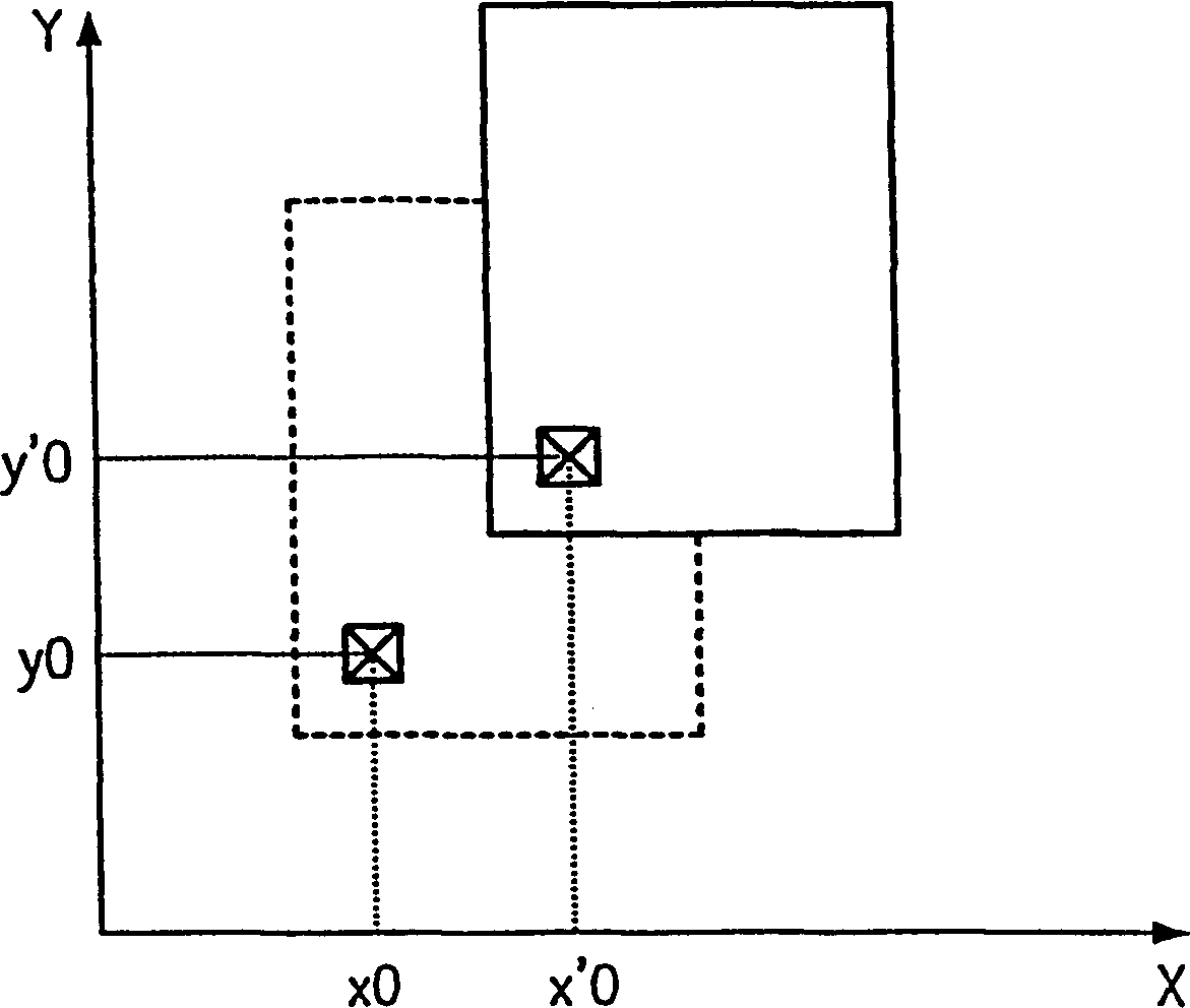
[0051] The parallel tester 2 has a main body 7 with a mounting area 8 on the top for fixing a printed circuit board to be tested. When both sides of the circuit board are to be tested, the mounting area 8 is provided with an adapter having contact elements for contacting the circuit board test points. Facing the mounting area...
PUM
 Abstract
Description
Claims
Application Information