

A non-radiative dielectric waveguide circuit positioned between two metal plates which are multi-layered for different seizes of spacers
A technology of waveguide circuits and dielectrics, which is applied in the direction of waveguides, circuits, waveguide devices, etc., and can solve the problem that semiconductors cannot be inserted
- Summary
- Abstract
- Description
- Claims
- Application Information
AI Technical Summary
Problems solved by technology
Method used
Image

Examples
Embodiment Construction
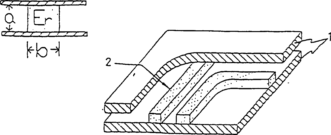
[0023] The most notable feature of the present invention is that a single circuit has non-radiating dielectric waveguides of different sizes, each size of waveguide producing a corresponding frequency. Another feature is that there are spacers of different heights between the two plates to allow each of the different non-radiating dielectric waveguides to fit properly. Doing this allows us to handle more than one frequency in a single circuit.
[0024] It will be helpful to understand the objects, features and advantages of the invention to study the embodiments of the invention with reference to the accompanying drawings. Figure 4 A non-radiating dielectric waveguide having the features described above is shown. As can be seen in this figure, the stacked metal plates (10, 11) allow a variety of spacers between them, so that a variety of non-radiating dielectric waveguides (20, 21) of different sizes can be inserted between the metal plates so that different frequencies can...
PUM
 Abstract
Description
Claims
Application Information