
Digital-to-analogue converting apparatus and method

A technology of digital-to-analog conversion and digital signal conversion, which is applied in the field of digital-to-analog conversion devices and can solve problems such as enlarged area

Inactive Publication Date: 2003-11-12
旭宏通讯股份有限公司
View PDF0 Cites 9 Cited by
  • Summary
  • Abstract
  • Description
  • Claims
  • Application Information

AI Technical Summary

Problems solved by technology

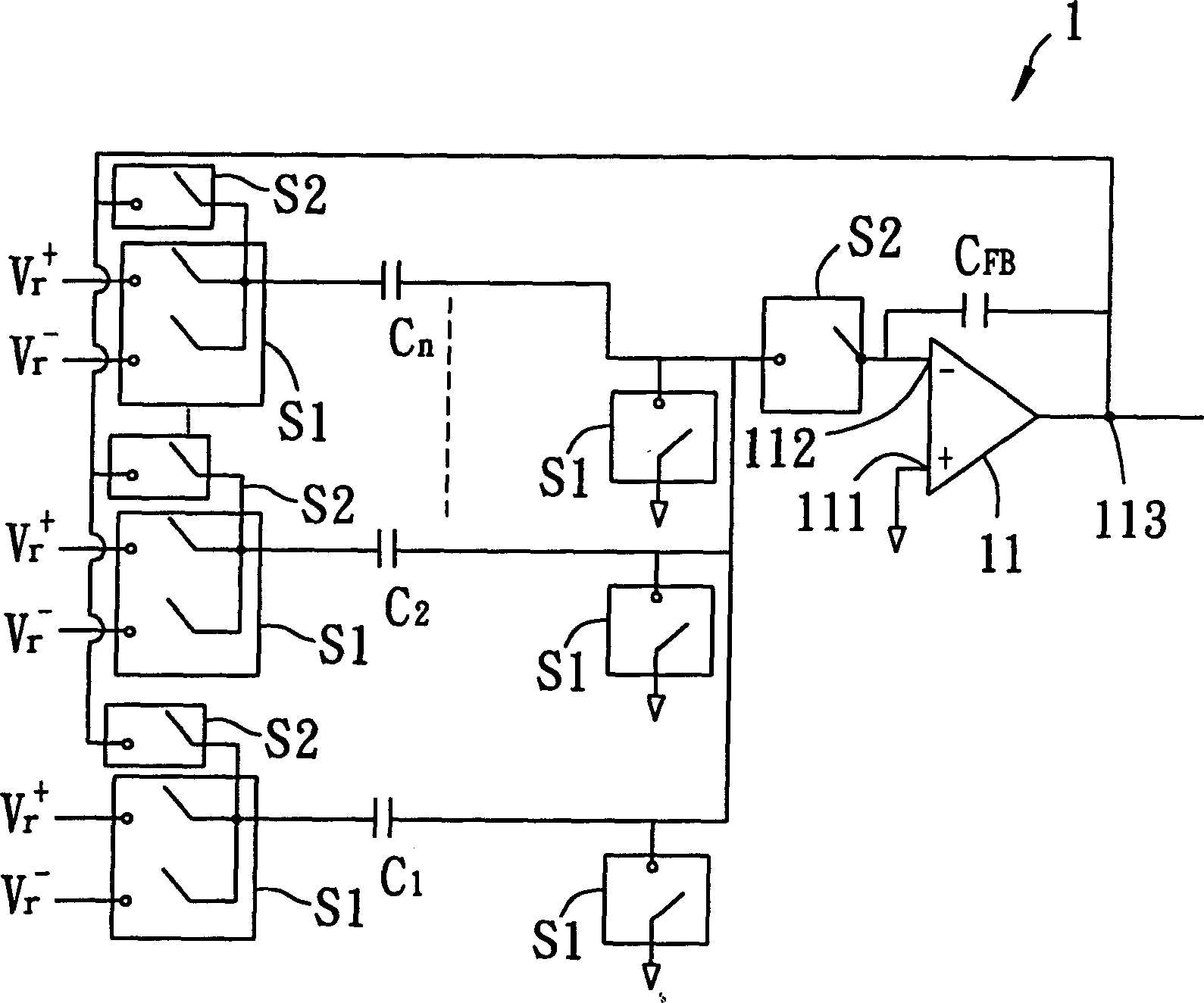
Utilize the two high logic levels of the first time period and the second time period that are completely opposite to the two time periods to control the digital-to-analog conversion action. When the first time period enters the high logic level, all the first switches S1 enter In the closed state, the first switch S1 is connected to a positive reference voltage or a negative reference voltage, and each bit captured by the first switch S1 is a high logic level (i.e. 1), then it is connected to a positive reference voltage, relatively If the bit captured by the ground is a low logic level (i.e. 0), it is connected to a negative reference voltage, so that each of the capacitors C1, C2, ..., Cn is charged with the amount of charge corresponding to the reference voltage of each bit, and then, When the second time period enters a high logic level, the first switch S1 is in the open state, and the second switch S2 is in the closed state, so that the capacitors C1, C2, ..., Cn and the feedback capacitor C FB It is connected in parallel between the negative input terminal 112 and the output terminal 113 of the operational amplifier 11, and according to the law of conservation of charge, the charge Q is redistributed between the capacitors C1, C2, ..., Cn and the feedback capacitor C FB However, the above-mentioned digital converter can only perform one-order conversion. If the above-mentioned device is used to expand to complete the high-order filter effect, the setting of the -3DB low-frequency cut-off frequency On the other hand, the capacitance value of the feedback capacitor CFB will be relatively increased, resulting in a larger area

Method used


Image

  • Digital-to-analogue converting apparatus and method
  • Digital-to-analogue converting apparatus and method
  • Digital-to-analogue converting apparatus and method

Examples


Embodiment Construction

[0035] As shown in circle 4, the digital-to-analog conversion device 3 of the first embodiment includes: an operational amplifier 31, n first capacitors C1, C2, ..., Cn, a second capacitor Ci, several switches Si and Sj, digital A first switch Sa, and two second switches S1, S2, the operational amplifier 31 has a short-circuited positive input terminal 311, a negative input terminal 312, an output terminal 313, and is connected between the negative input terminal 312 and the output terminal The feedback capacitor CFB between 313, the switch Sj is connected to the right end of each of the first capacitors C1, C2, ..., Cn, and the two ends of the second capacitor Ci, the switch Si is connected to each of the first capacitors C1, C2 , ..., the left end of Cn, the switch Si is to connect the left end of each of the first capacitors C1, C2, ..., Cn to two reference voltages of a reference voltage Vr+ or Vr-, wherein the voltage value of the reference voltage Vr+ is greater than The...


PUM


Abstract

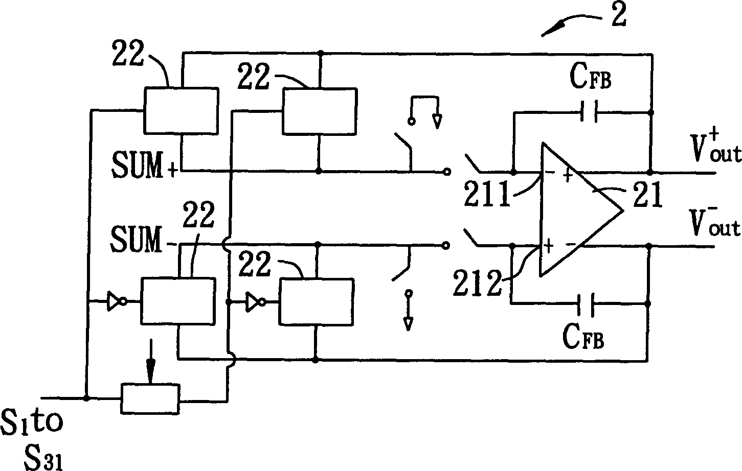
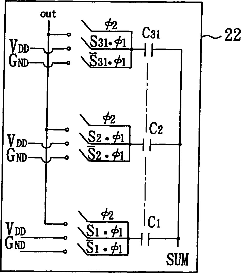
A device used to convert digital signal into analog signal comprises an operation amplifier, a first capacitor set, a second capacity, set, a first switch set and a second switch set. In the first time period, reference voltages corresponded by multiple bit in digital signal are transmitted respectively to the first capacity set; in the second time period, the second capacity set is connected to the first capacity set as the first switch set is closed and in the third time period, the second capacity set is connected between input end and output end of the operation amplifier as the second switch set is closed.

Description

(1) Technical field [0001] The present invention relates to a digital-to-analog conversion device and method, in particular to a digital-to-analog conversion device and method capable of performing more than one-order digital-to-analog conversion to achieve the effect of a higher-order low-pass filter. (2) Background technology [0002] Such as figure 1 As shown, the digital-to-analog conversion device 1 includes an operational amplifier 11, n capacitors C1, C2, ..., Cn, several first switches S1, and several second switches S2. The operational amplifier 11 has a short-circuit positive Input terminal 111, a negative input terminal 112, an output terminal 113, and a feedback capacitor CFB connected between the negative input terminal 112 and the output terminal, each of the left ends of the capacitors C1, C2, ..., Cn is connected to a first switch S2, and the right ends of the capacitors C1, C2, ..., Cn are also connected to the first switch S1, and the right ends of the cap...

Claims


Application Information

Patent Timeline
IPC IPC(8): H03M1/66
Inventor 郑铭福
Owner 旭宏通讯股份有限公司
Learn More