Method for forming wiring structure
A wiring structure and wiring groove technology, which is applied in the manufacture of electrical components, electrical solid devices, semiconductor/solid devices, etc., can solve problems such as surface cracks and cracks, and achieve the effect of preventing the deterioration of electromigration resistance
- Summary
- Abstract
- Description
- Claims
- Application Information
AI Technical Summary
Problems solved by technology
Method used
Image
Examples
Embodiment 1
[0055] Hereinafter, a method of manufacturing an electronic device according to Embodiment 1 of the present invention will be described with reference to the drawings. The present embodiment is characterized in that the Cu film is annealed between the CMP process of the copper (Cu) film as the wiring and the CMP process of the barrier film.
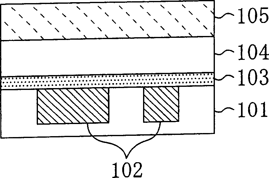
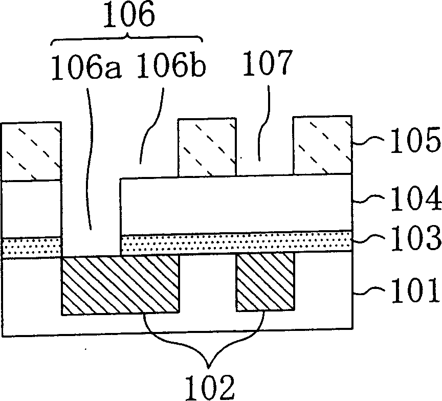
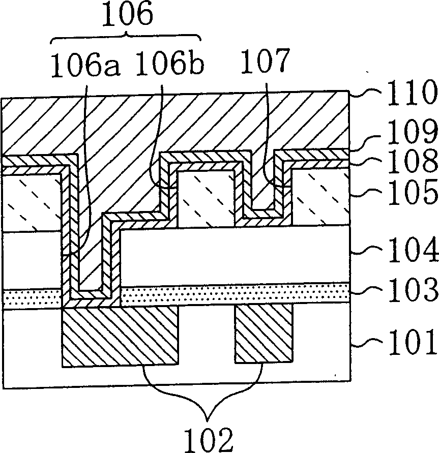
[0056] figure 1 ˜ FIG. 7 are cross-sectional views showing each step of the method of manufacturing the electronic device according to the first embodiment.
[0057] First, if figure 1 As shown, for example, after forming the lower wiring layer 102 inside the insulating film 101 deposited on a semiconductor substrate (not shown), the surface of the insulating film 101 buried in the lower wiring layer 102 is planarized. Then, on the planarized insulating film 101 and the lower wiring layer 102, for example, SiN film 103, SiO 2 film 104 and FSG film 105.
[0058] Then as figure 2 As shown, the SiN film 103, SiO 2 Recesses 106 and w...
Embodiment 2
[0079] Hereinafter, a method of manufacturing an electronic device according to Embodiment 2 of the present invention will be described with reference to the drawings. The present embodiment is characterized in that the CMP (Cu-CMP) process of the Cu film serving as wiring is performed twice, and at the same time, the Cu film is annealed between the Cu-CMP processes.
[0080] Figure 10 (a)-(d) are sectional views which show each process of the manufacturing method of the electronic device of Example 2.
[0081] First, with Example 1 (refer to Figure 1~3 ) same as Figure 10 As shown in (a), for example, after forming the lower wiring layer 102 inside the insulating film 101 deposited on a semiconductor substrate (not shown), the surface of the insulating film 101 buried in the lower wiring layer 102 is planarized. Then, on the planarized insulating film 101 and the lower wiring layer 102, for example, SiN film 103, SiO, and SiO are sequentially deposited by CVD. 2 film 1...
Embodiment 3
[0093] Hereinafter, a method of manufacturing an electronic device according to Embodiment 3 of the present invention will be described with reference to the drawings. The present embodiment is characterized in that after the CMP process for the Cu film and the barrier film as wirings, the Cu film is annealed, and thereafter, at least one CMP process capable of shaving off the Cu film is performed.
[0094] Figure 11 (a)-(d) are sectional views which show each process of the manufacturing method of the electronic device of Example 3.
[0095] First, with Example 1 (refer to Figure 1~3 ) same as Figure 11 As shown in (a), for example, after forming the lower wiring layer 102 inside the insulating film 101 deposited on a semiconductor substrate (not shown), the surface of the insulating film 101 buried in the lower wiring layer 102 is planarized. Then, on the planarized insulating film 101 and the lower wiring layer 102, for example, SiN film 103, SiO 2 film 104 and FSG f...
PUM
 Abstract
Description
Claims
Application Information


