

Semiconductor device
A technology for semiconductors and devices, applied in the field of semiconductor devices, can solve the problems of upper-layer wiring disconnection, disconnection, high reliability obstacles of semiconductor devices, etc.
- Summary
- Abstract
- Description
- Claims
- Application Information
AI Technical Summary
Problems solved by technology
Method used
Image

Examples
Embodiment 1
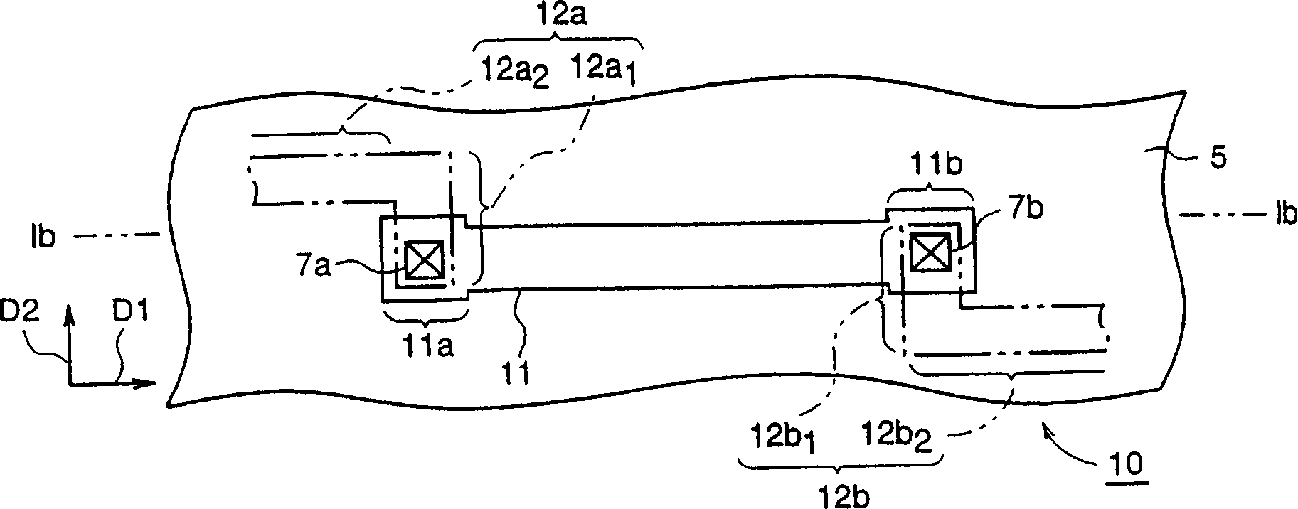
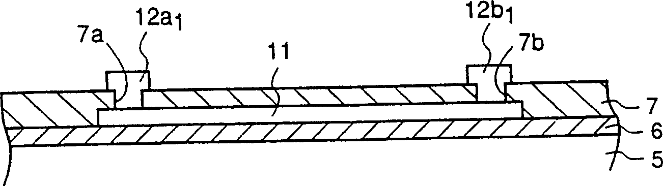
[0062] Fig. 1 is the figure for explaining the semiconductor device of embodiment 1 of the present invention, and the plan view of Fig. 1 (a) has shown the wiring structure of the semiconductor device of embodiment 1 of the present invention, and Fig. 1 (b) is its Ib- Ib line profile.
[0063] In the figure, 10 is a wiring structure of a semiconductor device. This wiring structure 10 has a lower layer wiring (first wiring) 11 extending in a first direction and having a second direction perpendicular to the first direction as a wiring width direction, and in which tensile stress (thermal stress) has been generated inside, and The upper layer wirings (second wirings) 12 a and 12 b are electrically connected to the lower layer wiring 11 and are affected by the thermal stress of the lower layer wiring 11 .
[0064] Among them, the above-mentioned lower layer wiring 11 is formed by patterning a platinum layer formed on the silicon substrate 5 through the base insulating film 6, an...
Embodiment 2
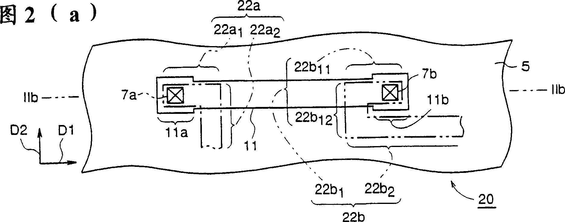
[0070] Fig. 2 is the figure for explaining the semiconductor device of embodiment 2 of the present invention, the plan view of Fig. 2 (a) has shown the wiring structure of the semiconductor device of embodiment 2 of the present invention, Fig. 2 (b) is its IIb- Sectional view of line IIb.
[0071] In the figure, 20 is the wiring structure of the semiconductor device of the second embodiment. This wiring structure 20, like the above-mentioned first embodiment, includes a lower layer in which tensile stress (thermal stress) has been generated inside, extending in the first direction D1 and having a second direction perpendicular to the first direction as the wiring width direction. Wiring (first wiring) 11, and upper wiring (second wiring) 22a, 22b electrically connected to lower wiring 11 and affected by thermal stress of lower wiring 11. FIG.
[0072] The above-mentioned upper layer wirings 22a and 22b are formed by patterning an aluminum layer formed on the platinum layer co...
Embodiment 3
[0078] 3 is a plan view for explaining a semiconductor device according to Embodiment 3 of the present invention, and shows a wiring structure of the semiconductor device.
[0079] In the figure, 30 is the wiring structure of the semiconductor device of the third embodiment. Its cross-sectional structure is the same as the wiring structure in the conventional wiring structure 250 of a semiconductor device. This wiring structure 30 has a lower layer wiring (first wiring) 31 in which tensile stress (thermal stress) has been generated, and an upper layer wiring (first wiring) electrically connected to the lower layer wiring 31 and affected by the thermal stress of the lower layer wiring 31 2nd wiring) 2a, 2b.
[0080] Among them, the above-mentioned lower layer wiring 31 is formed by patterning a platinum layer formed on the silicon substrate 5 through an insulating film, and one top end 31a thereof is connected to the above-mentioned upper layer through a contact hole 7a formed...
PUM
 Abstract
Description
Claims
Application Information