Signal transmission structure

A signal transmission and reference plane technology, applied in the direction of semiconductor/solid-state device components, semiconductor devices, electrical components, etc., can solve the impedance mismatch, the signal cannot be completely transmitted from a signal transceiver, the insertion loss becomes larger, etc. achieve the effect of improving integrity

Inactive Publication Date: 2004-02-25
VIA TECH INC
View PDF0 Cites 7 Cited by
  • Summary
  • Abstract
  • Description
  • Claims
  • Application Information

AI Technical Summary

Problems solved by technology

[0005] Please refer to Figure 1A , Figure 1B , when the signal passes through the conductive wire 130, the bonding pad 120, the conductive ball 140, the bonding pad 12a and the conductive wire 12b, due to the geometry of the conductive ball 140 itself, a discontinuous low voltage is generated between the conductive ball 140 and the reference plane 110 Impedance characteristics, thus resulting in the phenomenon of impedance mismatch in the adjacent signal path of the conductive ball 140
Therefore, when the signal passes through the adjacent signal path of the conductive ball 140, the signal will be reflected, resulting in that the signal cannot be completely transmitted from one signal receiving end to another signal receiving end through the conductive ball 140.
In addition, as the operating frequency of the signal increases, when the signal passes through the conductive ball 140, the return loss of the signal will become relatively smaller, and the insertion loss of the signal will also become relatively obvious. Large, so that the degree of impedance mismatch in the adjacent signal path of the conductive ball 140 is more obvious, which is quite unfavorable for the transmission of high-frequency signals

Method used


Image

  • Signal transmission structure
  • Signal transmission structure
  • Signal transmission structure

Examples


no. 1 example

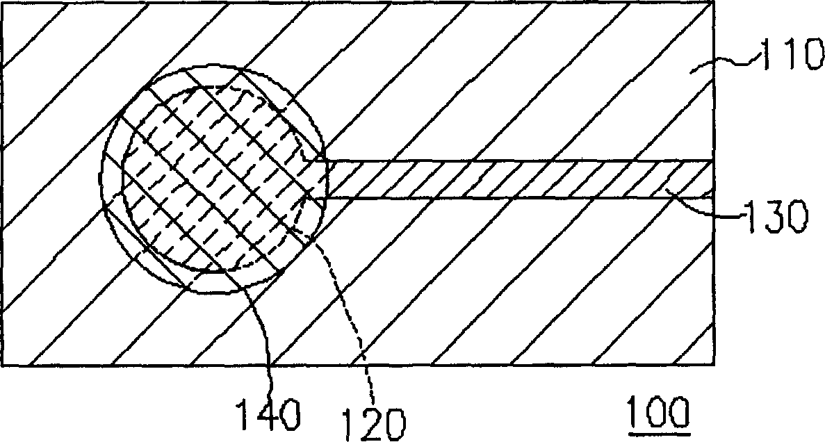
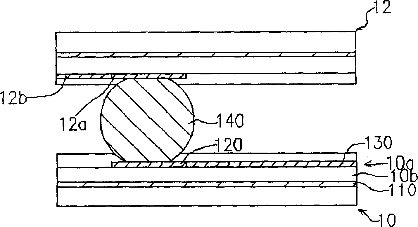
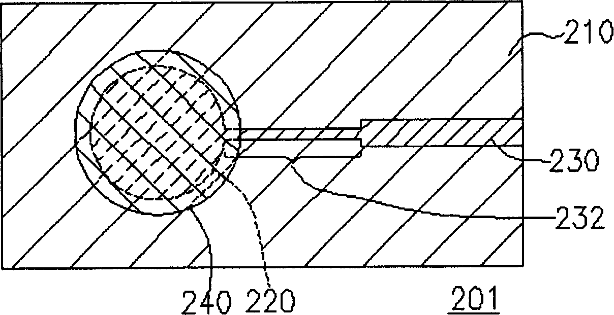
[0045] Please refer to Figure 2A , Figure 2B ,in Figure 2Arepresents a top view of a signal transmission structure of the first embodiment of the present invention, and Figure 2B express Figure 2A A cross-sectional view of a signal transmission structure applied to a signal transmission medium. The signal transmission structure 201 is suitable for a signal transmission medium 20 (such as a printed circuit board). The signal transmission structure 201 includes a reference plane 210 , a bonding pad 220 , a conductive trace 230 and a conductive ball 240 . The reference plane 210 is, for example, a ground plane or a power plane, which is buried inside the signal transmission medium 20, while the bonding pads 220 and the wires 230 are circuit patterns on the surface of the signal transmission medium 20. pattern) 20a, and the bonding pad 220 and the wire 230 are electrically isolated from the reference plane 210 by a dielectric layer 20b, so the bonding pad 220 and the wir...

no. 2 example

[0051] Compared with the above-mentioned first embodiment, the second embodiment forms a non-reference area (such as an opening) on ​​the reference plane, and the position of this non-reference area corresponds to the position of the adjacent part of the above-mentioned wire, so as to The equivalent inductance between the adjacent part of the wire and the reference plane is increased to compensate for the high equivalent capacitance between the conductive ball and the reference plane, so that the conductive ball and its adjacent signal path have better impedance matching.

[0052] Please refer to Figure 3A , Figure 3B ,in Figure 3A represents a top view of a signal transmission structure of the second embodiment of the present invention, and Figure 3B express Figure 3A A cross-sectional view of a signal transmission structure applied to a signal transmission medium. The signal transmission structure 202 of the second embodiment also includes a reference plane 210 , a ...

no. 3 example

[0054] Compared with the above-mentioned second embodiment, the third embodiment also forms a non-reference area (such as an opening) on ​​the reference plane, but the position of the non-reference area corresponds to the position of the conductive ball to improve the conductive ball. The equivalent inductance between the conductive ball and the reference plane (that is, reducing the equivalent capacitance between the conductive ball and the reference plane) enables the conductive ball to have better impedance matching with its adjacent signal path.

[0055] Please refer to Figure 4A , Figure 4B ,in Figure 4A shows a top view of a signal transmission structure of the third embodiment of the present invention, and Figure 4B express Figure 4A A cross-sectional view of a signal transmission structure applied to a signal transmission medium. The signal transmission structure 203 of the third embodiment also includes a reference plane 210 , a bonding pad 220 , a wire 230 a...


PUM


Abstract

The present invention relates to a signal transmission structure, mainly including reference plane, combination pad, conductive wire and conductive ball. The signal transmission structure utilizes the change of the form of the reference plane or conductive wire to relatively reduce the equivalent capacity of thue conductive ball and its adjacent signal path or relatively raise the equivalent induction of the conductive ball and its adjacent signal path so as to compensate the high equivalent capacity between the conductive ball and reference plane, and can make the conductive ball and its adjacent signal path have the better impedance matching to raise the completeness of the signal after which is passed through the conductive ball and its adjacent signal path.

Description

technical field [0001] The present invention relates to a signal transmission structure, and more particularly to a signal transmission structure suitable for a signal transmission medium for improving the impedance mismatch of a signal transmission path. Background technique [0002] With the rapid development of the electronic technology industry, various electronic products with different functions have gradually penetrated into our work and life. Electronic products are usually equipped with a motherboard, which includes a circuit board and a plurality of electronic components, and these electronic components are assembled on the circuit board and electrically connected to each other through the internal circuits of the circuit carrier board to provide electronic products. The designed function, wherein these electronic components also include integrated circuit (Integrated Circuit, IC for short) components. In order to effectively protect the fragile IC die and at the ...

Claims


Application Information

Patent Timeline
Patent Type & Authority Applications(China)
IPC IPC(8): H01L23/48H05K3/32
CPCH01L2224/16
Inventor 徐鑫洲
Owner VIA TECH INC
Why Eureka
Try Eureka