High radiation miniature package for semiconductor chip

A technology of high heat dissipation and packaging, which is applied in the direction of semiconductor devices, semiconductor/solid-state device components, electric solid-state devices, etc., and can solve the problems that the volume of packages cannot be effectively reduced

Inactive Publication Date: 2004-03-24
ORIENT SEMICON ELECTRONICS
View PDF0 Cites 5 Cited by
  • Summary
  • Abstract
  • Description
  • Claims
  • Application Information

AI Technical Summary

Problems solved by technology

However, in this method, since the chip 2' must be placed below the entire package, the size of the chip and the location of the bonding wire must be considered when designing the solder ball 12' on the surface of the substrate 1', so that the entire package cannot be effectively reduced. volume of

Method used


Image

  • High radiation miniature package for semiconductor chip
  • High radiation miniature package for semiconductor chip
  • High radiation miniature package for semiconductor chip

Examples


Embodiment Construction

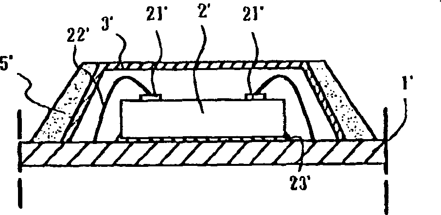
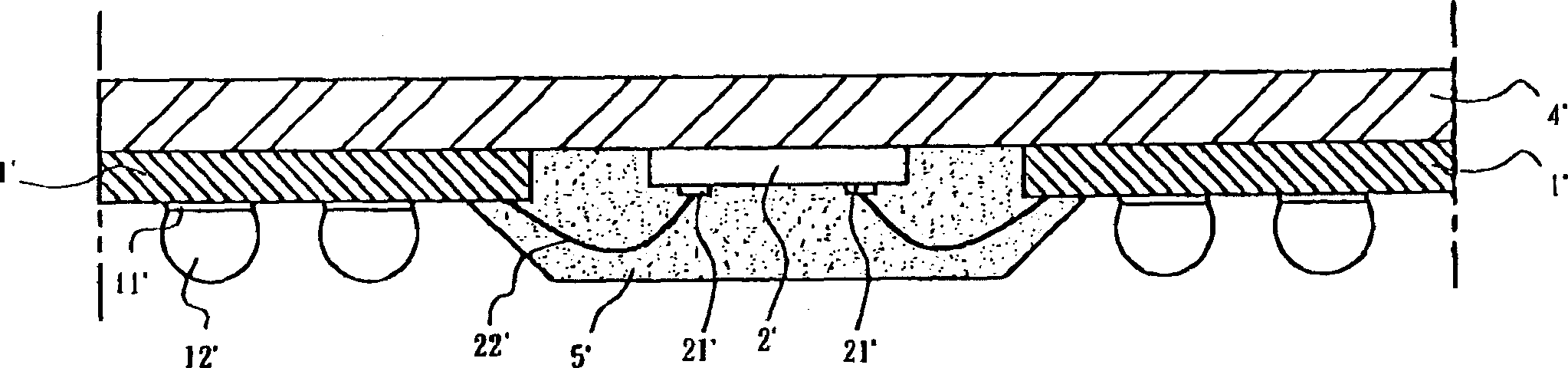
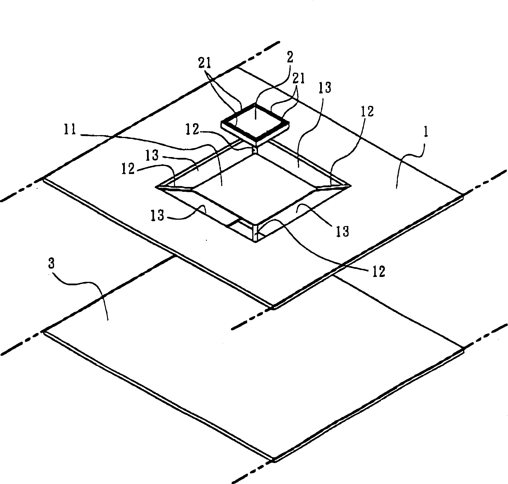
[0017] See first image 3 , Figure 4 As shown, the high heat dissipation tiny package body of the semiconductor chip of the present invention comprises:

[0018] A lead frame 1, the lead frame 1 produces a platform of a recessed chip holder 11 by an etching process, and hollow hollow slots 13 are set around the chip holder 11, leaving only a few supporting strips 12 connected to the lead frame main body ;

[0019] A substrate 3, the substrate 3 can be applied to the production of high-density circuits to meet the requirements of high pin count, the substrate 3 is attached to the bottom of the lead frame 1, and the substrate 3 is provided with high-density circuits and a large number of foot pads 31 and solder balls 32, and make the pads 31 in the hollow slot 13 relative to the lead frame 1, so as to join the gold wires 22;

[0020] A chip 2, the chip 2 is positively bonded to the chip holder 11 of the lead frame 1 with the bonding agent 23, and the gold wire 22 is placed o...


PUM


Abstract

A high radiation micropackaged device of a semiconductor chip includes a wire frame and a base board, among which, a concave platform chip seat is set at the center of the frame with engraved slottedeyes surrounding it, only several supporting plates connecting the seat to the frame, high density circuit and multiple pads and tin balls, a chip joining to the top of the seat of the frame with a binding agent, combining the chip pads and the base board pads with metal wires and filling glue into the engraved slotted eyes, wrapping the metal wires and part surfaces of the frame.

Description

【Technical field】 [0001] The invention relates to a packaging body of a semiconductor chip, in particular to a micro packaging body of a semiconductor chip with high heat dissipation. 【Background technique】 [0002] Generally speaking, in the known three-dimensional packaging technology of semiconductor chips, common figure 1 The structure shown is generally applied to TEBGA, IIQFP, etc., and its main structural feature is to bond a chip 2' with a bonding agent 23' on a substrate 1', and then bond it to the foot pad 21 of the chip 2' by wire bonding technology. The chip 2' and the substrate 1' are bonded to each other with gold wires 22', and the chip 2' and its gold wires 22' are covered with a cooling plate 3', and then encapsulated with a sealant 5' around the cooling plate 3'. Since this method must add a heat sink 3' outside the chip 2', it cannot achieve the goal of being small and thin. [0003] Another idiom such as figure 2 As shown, it is generally used in EBGA...

Claims


Application Information

Patent Timeline
Patent Type & Authority Applications(China)
IPC IPC(8): H01L23/12H01L23/28H01L23/495
CPCH01L2224/45144H01L2224/48091H01L2224/73265
Inventor 谢文乐杨家铭梁淑芬谢岩树周淑敏
Owner ORIENT SEMICON ELECTRONICS
Why Eureka
Try Eureka